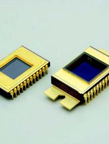
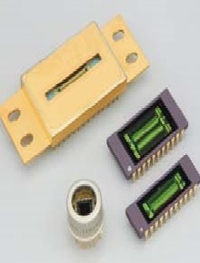
NMOS linear image sensor
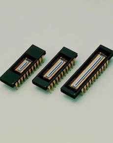
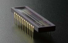
CCD linear image sensor
CMOS linear images sensor
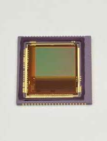
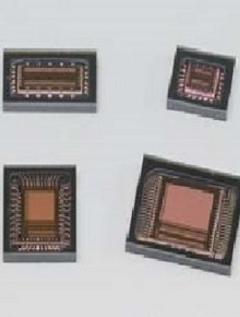
Front-illuminated type CCD area image sensor
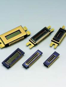
CMOS area image sensor
Back-thinned type CCD area image sensor
X-ray image sensor
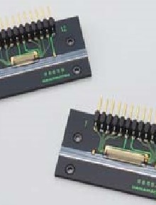
Multichannel detector head
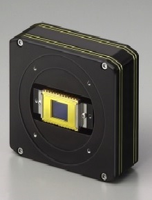
Image Sensors for Near Infrared Region
Distance image sensors
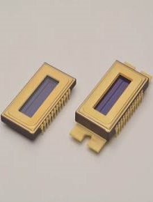
Photodiode Arrays with Amplifier
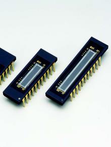
Back-thinned TDI
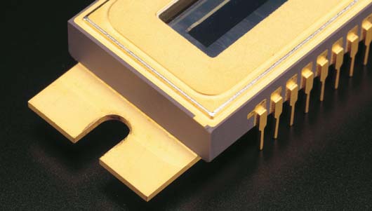
Back-thinned TDI (time delay integration)-CCDs allow acquiring high S/N images even under low-light conditions during high-speed imaging and the like. TDI operation yields dramatically enhanced sensitivity by integrating the exposure of a moving object. The back-thinned structure ensures high quantum efficiency over a wide spectral range from the ultraviolet to the near infrared region (200 to 1100 nm).
FFT-CCD area image sensor
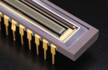
Image Sensor
Back-thinned TDI (time delay integration)-CCDs allow acquiring high S/N images even under low-light conditions during high-speed imaging and the like. TDI operation yields dramatically enhanced sensitivity by integrating the exposure of a moving object. The back-thinned structure ensures high quantum efficiency over a wide spectral range from the ultraviolet to the near infrared region (200 to 1100 nm).
![]() +886-2-8772-8910
+886-2-8772-8910