- HOME
- 產品介紹
- 半導體事業部
- Hamamatsu Photonics
- Image Sensor
- FFT-CCD area image sensor
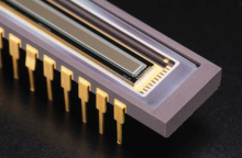
FFT-CCD area image sensor
![]() +886-2-8772-8910
+886-2-8772-8910
Characteristics and use of FFT-CCD area image sensor
1. CCD image sensor overview
CCD area image sensors are semiconductor devices invented by Boyle and Smith at the AT&T Laboratory in 1970.
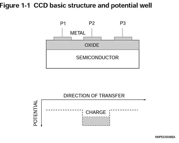
The CCD (Charge-Coupled Device) comes from operation/ function that charge stored in one area of the CCD is transferred (or coupled) to an adjacent area. Areas where the charge is stored are referred to as potential wells, and are created when an external voltage is applied to the gate electrodes. The struc- ture of a CCD is based upon a MOS (Metal Oxide Semiconduc- tor) capacitor (Figure 1-1). The gate electrodes (P1, P2 and P3) are usually made from a highly conductive material such as metal or polysilicon. The oxide layer is SiO2 (silicon dioxide) and the channel is a semiconductor.
CCDs are grouped within a family of charge transfer devices (CTDs) that utilize so-called potential wells to transfer an accu- mulated charge through the semiconductor. Most current CCDs
have a buried channel CCD (BCCD) structure, in which the charge transfer channel is embedded inside the substrate.
Groups of gate electrodes form a single pixel in the CCD. In Figure 1-1 there are 3 electrodes needed to form one pixel, and these electrodes are grouped into other sets (2 or 4) to create a pixel. When a series of pixels are fabricated, they form a CCD register. CCDs are comprised of 3 sections; a vertical register, horizontal register and an amplifier or output stage. The vertical register is a series of photosensitive columns (64, 128 or 256 pixels, etc.) which transports charge to the horizontal register. The horizontal register transports charge to an on chip amplifier which converts the charge to a voltage.
As shown in Figure 1-1, a potential well is created beneath P2 when positive voltage is applied to P2, while the voltages ap- plied to P1 and P3 are zero. This difference in the electrical potential creates a potential barrier in which electrons are con- fined. By adjusting these voltages in the appropriate time se- quence, the signal charge packed in this potential well is se- quentially transferred through the semiconductor toward the output section. Because of this, the CCD is often likened to an analog shift register as compared with a digital shift register. CCDs are essentially semiconductor devices through which a signal charge is transferred. Recently, however the term “CCD” has come to signify image sensors and even video cameras, since CCDs are preferred in a wide range of imaging applica- tions. Throughout the remainder of this paper, CCD refers to an image sensor, not merely transfer devices.
1-1 CCD area image sensor types and operat- ing principles
Current used CCD area image sensors are classified by their transfer methods into the following 4 types:
(1) Frame Transfer (FT)
(2) Full Frame Transfer (FFT)
(3) Interline Transfer (IT)
(4) Frame Interline Transfer (FIT)
These 4 configurations (except for the FFT-CCD) are widely used in general purpose video cameras. The FFT-CCD, be- cause of its operating principle, is not well suited for use in video cameras. FFT-CCD is primarily used in measurement applications such as spectrophotometry, where it is important to make quantitative measurements.
(1) Frame Transfer (FT)
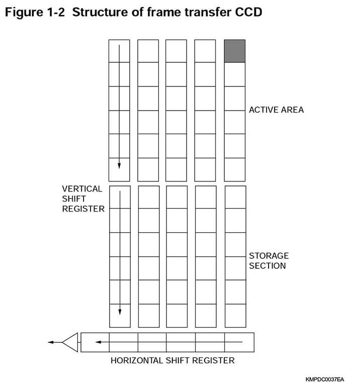
Frame transfer CCDs are comprised of two vertical shift regis- ters used, in the photosensitive and storage sections respec- tively, one horizontal shift register, and an output section. Transparent electrodes, such as polysilicon, are generally em- ployed as the metal electrodes in the photosensitive section. When light comes through a transparent electrode into the CCD semiconductor, photoelectric conversion generates a sig- nal charge. This signal charge collects into the potential well beneath the electrode. By utilizing the vertical blanking period, this charge is transferred at high speed to the storage section for each frame. Thus, the vertical shift register in the photosen- sitive section of the frame transfer acts as a photoelectric con- verter during the signal integration period. The storage section performs signal transfer to the output sec- tion through the horizontal shift register. Photoelectric conver- sion and signal accumulation take place in the photosensitive section. The signal charge is transferred to the horizontal shift register for each line in the storage section during the horizon- tal blanking period.
In the frame transfer type, all areas other than the photosensi-tive section are covered with an opaque metal, such as alumi- num, that prevents light from entering. Figure 1-2 shows a simplified structure of a frame transfer CCD.
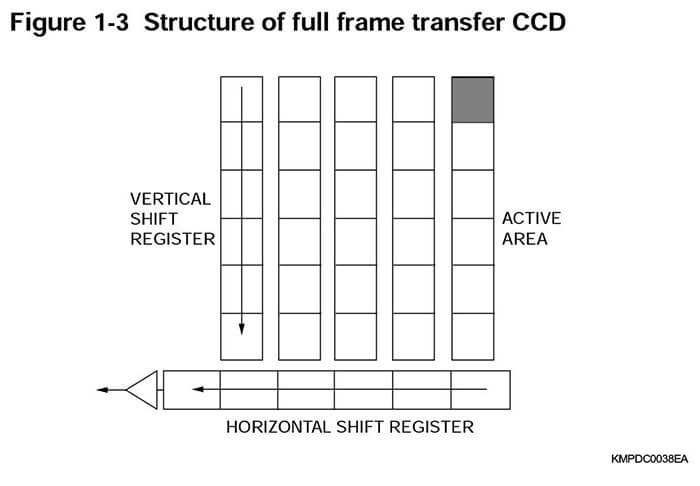
(2) Full Frame Transfer (FFT)
The FFT-CCD basically has the same structure as frame trans- fer CCDs, except the storage section is removed. Because there is no storage section, the FFT-CCD is usually used in conjunction with some form of external shutter mechanism. This limitation makes it difficult to use the FFT-CCD as a video cam- era.
The operating principle of the FFT-CCD is quite similar to that of the frame transfer CCDs. The signal charge is collected in a potential well in the photosensitive section during the signal integration period, then transferred to the output section via the horizontal shift register during the closed period of an external shutter.
Since a storage section is not provided, the FFT-CCD can be fabricated with a larger number of pixels of the same size or with a larger active area per pixel. This makes the FFT-CCD well suited for scientific applications where a slow frame rate is de- sired. Hamamatsu CCDs are FFT-CCD. A simplified structure of a FFT-CCD is shown in Figure 1-3.
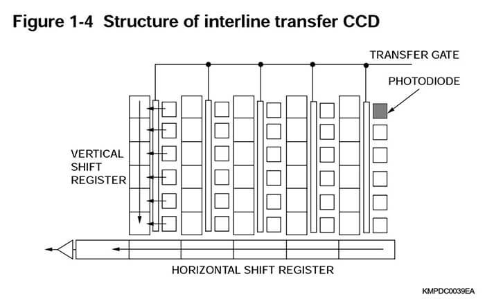
(3) Interline Transfer (IT)
Interline transfer CCDs have a photosensitive section consist- ing of photodiodes and MOS structure diodes formed sepa- rately from the transfer section. Most devices use buried photo- diodes with a low dark current. Vertical shift registers are ar- ranged along photodiode arrays so as to enclose each photo- diode. Vertical shift registers are comprised of respective output sections that also include a horizontal shift register.
The signal charge produced by photoelectric conversion in a photodiode is stored in the photodiode junction capacitance. This charge is then transferred to the vertical shift register dur-ing the vertical blanking period through the transfer gate. The transfer gate is an analog switch which is between the vertical shift register and the photodiode array. This operation differs from frame transfer CCDs in that charge transfer from the photo- diode to the vertical shift register is performed for all pixels si- multaneously.
Subsequent operations are exactly the same as frame transfer CCD. That is, the signal charge is transferred to the horizontal shift register for every line during the horizontal blanking period. As with frame transfer CCDs, all areas other than photodiodes are covered with an opaque metal, such as aluminum, to achieve light shielding.
Figure 1-4 shows the simplified structure of an interline transfer CCD.
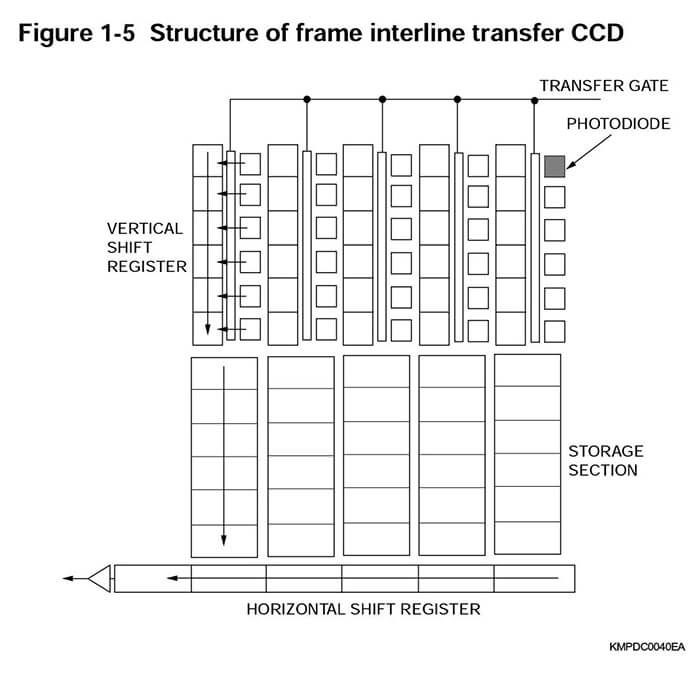
(4) Frame Interline Transfer (FIT)
Frame interline transfer CCDs were developed to solve prob- lems of interline transfer CCDs. FIT-CCD are configured with an added storage section. In interline transfer CCDs, after the charge from the photodiode is transferred to the vertical regis- ter, the vertical register is clocked and the photodiode accumu- lates the next signal charge. With so many optically generated carriers in close proximity to the vertical shift register, signals leak into the vertical register. This phenomenon is known as “smear”. To solve the smear problem, the frame interline trans- fer CCD transfers the signal charge to the storage section at a high speed as soon as the vertical shift register receives the signal charge from the photodiode. Therefore, the frame inter- line transfer CCD ensures reduced smear as compared with the interline transfer CCD.
A simplified structure of a frame interline transfer CCD is shown in Figure 1-5.
Figure 1-2 Structure of frame transfer CCD
1-2 CCD linear image sensor types and operat- ing principles
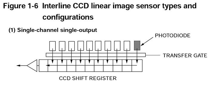
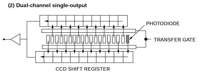
Interline CCD linear image sensors contain photosensitive sec- tion comprised of P-N junction photodiodes arrayed in a row. A signal charge produced by photoelectric conversion in each photodiode accumulates as an internal capacitance. The pho- toelectric conversion and the resulting charge accumulation are performed over a period of time, and the accumulated charge is transferred to the CCD shift register as the transfer gate is switched. The charge transfer from the photodiode to the shift register is performed for all pixels simultaneously. The sig- nal charge from each pixel is then sequentially transferred to the output section where it is converted into voltage by a charge amplifier. As a result, the signal is derived as an output voltage from the image sensor. The interline CCD is grouped by shift register and output con- figuration into the following three types:
(1) Single-channel single-output
(2) Dual-channel single-output
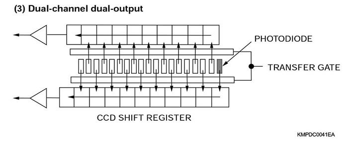
(3) Dual-channel dual-output
These three types are selected according to the sensor element pitch and signal frequency (data rate) that is required. CCDs with a sensor element pitch greater than 25 µm are used to transfer the signal charge by means of single-channel single- output. CCDs with an element pitch less than 25 µm are used as a dual-channel output type that transfers the signal charge with two shift registers provided along the sides of the photodiode array for odd and even bits, respectively. Further, a dual-chan- nel dual-output is used in applications requiring high-speed transfer. In this dual-channel dual-output, the odd and even bits should be combined at a latter-stage circuit of the CCD image sensor.
1-3 Charge transfer operation
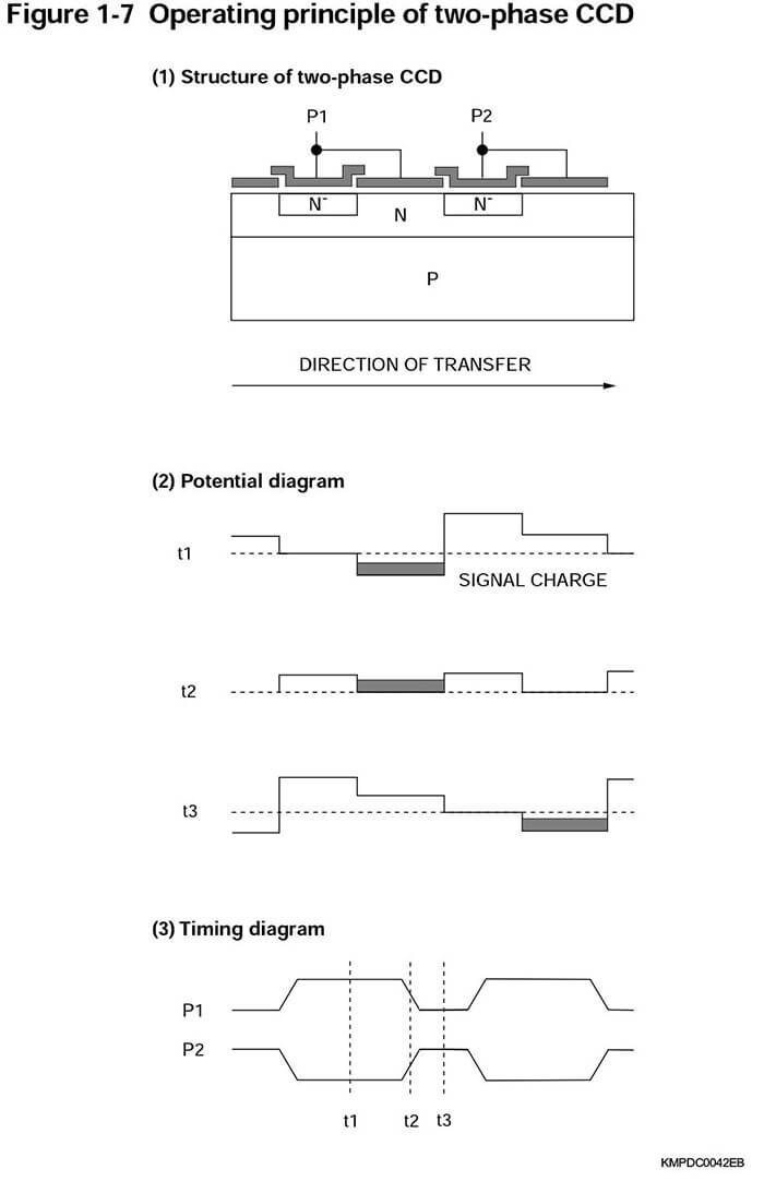
In charge transfer operations, CCDs using a pair of gate elec- trodes for one pixel are called two-gate CCDs or two-phase CCDs. Figure 1-7 shows the operating principle of a typical two- phase CCD in which the signal charge is transferred by apply- ing two clock pulses with different voltage levels; for example, VH (high level) and VL (low level) to the electrodes (P1 and P2 in the Figure 1-7). In a two-phase CCD, the signal charge is transferred in the direction determined by the potential difference created in wa- fer process. The signal charge is stored beneath the storage region, as shown in Figure 1-7 (2) Potential diagram.
For example, by setting electrode P1 to high level (P2 to low level) at the phase t1, the signal charge is stored beneath the storage electrode of electrode P1. Charge is confined under gate P1 by means of the potential applied to adjacent gates, implanted barrier and channel stops. Channel stops are highly doped regions perpendicular to electrodes P1 and P2 and help confine charge to the lateral direction. It is important for two-phase CCDs to optimize overlapping of clock pulses. As shown in the timing diagram Figure 1-7 (3), clock pulses must cross with each other (phase t2) at a level higher than the midpoint of the high and low levels (for example, if the high level is V and the low level is 0, cross point should be higher than V/2). Alternate switching of the high level state al- lows the charge to move in the direction of transfer.
At the phase t2, the potential of P1 is equal to P2, which is one- half of the applied electrode voltage (V). This causes the barrier beneath P2 to decrease and enables the formation of the next potential well. At the phase t3, P1 is zero, while P2 is at high level (V). The charge has moved from the collapsing potential well beneath P1 to P2.
1-4 Signal readout method
The signal charge transferred by the shift register is finally con- verted to a voltage corresponding to the charge in the output section.
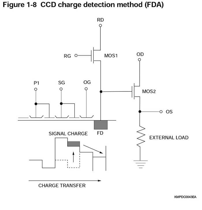
The most popular method for detecting the signal charge of a CCD is the floating diffusion amplifier (FDA) method (Figure 1- 8). This method consists of nodes for detecting a charge and a pair of MOSFETs connected to each node (MOS1 for reset and MOS2 for charge-to-voltage conversion). The charge trans- ferred to this detecting node is converted into a voltage by the MOSFET for charge-to-voltage conversion, with the relation Q=CV. This signal readout is performed nondestructively, but the detecting node is reset by MOS1 to the reference level (volt- age on RD), in order to read the next signal. Therefore, the FDA falls under the destructive readout method generally.
Noise resulting from this readout method is determined by the capacitance of the node (Cfd), but can be almost entirely elimi- nated by the correlated double sampling (CDS) as proposed by White.
The timing of the signal charge output is synchronized with the timing of the summing gate (SG), which is the last clock gate for the horizontal shift register. This signal appears when the gate is set to low.
1-5 Binning of signal charge
Binning is a unique operation of CCDs and is divided into two methods (line binning and pixel binning) depending on the di- rection of the signal charge.
(1) Line binning
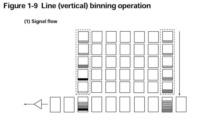
In CCD operation, a signal charge accumulates in the potential well of every pixel during the integration time. For FFT-CCDs, this means that the charge information is two-dimensionally stored at the end of the integration time as shown in Figure 1-9. Concurrently, the vertical and horizontal shift registers are fed with clock pulse separately, thus enabling the binning opera- tions described below. A method for summing the signal of each vertical pixel is re- ferred to as line binning or vertical binning. As shown in Figure 1-9, by applying a specified number of clock pulses to the verti- cal shift register with the horizontal shift register clocks P1H halted, the signal charge of each vertical pixel is sequentially transferred and added to each horizontal register. After the ver- tical binning of the Nth element is completed, the horizontal clocks are restarted and the signal is sent via the output stage to an external circuit.
This line binning operation provides the signal charge that is equivalent to the sensor having the same long active area. In addition, this enables you to read out the whole vertical signals at one time, thus minimizing the noise resulting from the signal readout process.
For low light level detection, the number of pixels in the vertical direction plays an important role in the signal to noise ratio. Since each pixel generates dark current, the more pixels in the vertical direction, the more dark current summed into the hori- zontal register.
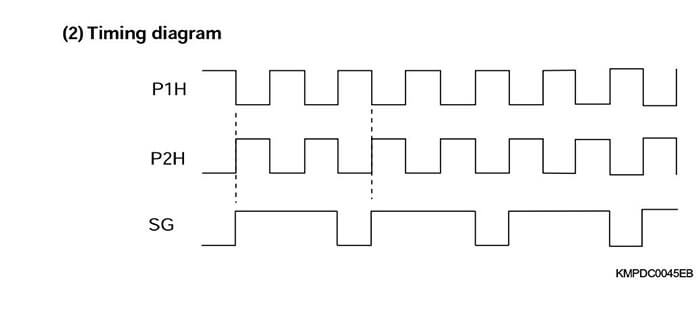
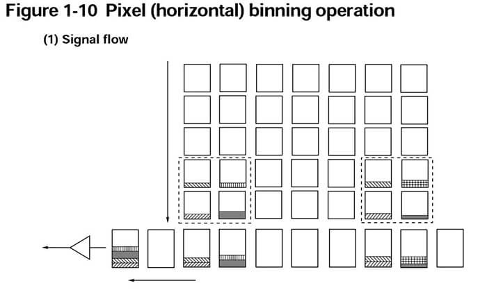
(2) Pixel binning
The summing gate (SG) is the last gate for the horizontal shift register. In normal operation, the summing gate is used as P2H. (The SG terminal can be handled as a separate terminal and fed with the same timing clock for P2H.)
Pixel binning or horizontal binning is performed by applying a clock pulse to the summing gate. For example, the signal from 2 × 2 pixels shown in Figure 1-10 is summed by combining with line binning. In this technique, the signals of two vertical lines are summed by line binning into the horizontal shift register. Next, as the horizontal shift register reads the signals of the two horizontal pixels, these signals can be summed to the summing well by applying only one clock pulse to the SG terminal, while two P1H clock pulses are applied to the P1H gate.
This technique ensures an image with higher contrast, but at the sacrifice of spatial resolution. For example, when CCD image sensor S7018-1010 is used at low light levels, improved image contrast is achieved by operating S7018-1010 as an image sensor with 512 × 512 pixels.
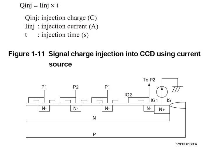
1-6 Signal charge injection
CCDs have input sources (ISV, ISH) and input gates (IGV, IGH) formed on the vertical shift register and horizontal shift register, respectively as signal input terminals for CCD electrical test. In most cases, a constant bias specified in the data sheet should be applied to these test terminals. However, by applying a bias other than the specified value, or clock, to these input sources and gates, a signal charge can be injected into the CCD shift registers. Injecting a bias charge (constant signal charge) into the CCD improves the transfer efficiency of CCDs that have suffered radiation damage. These terminals are also utilized to evaluate the saturation charge (full well capacity) and FDA (am-plifier) linearity.
To inject a signal charge into the CCD shift register, a current source should be connected to the input source, and the input gate should be shorted to P2 for clock operation. The signal charge injected by this method equals the product of the current source value and the injection time (reciprocal of CCD drive frequency).
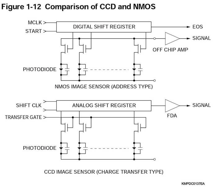
1-7 Comparison between CCD and NMOS image sensors
CCD and NMOS image sensors are different in terms of specifi- cations and performance. This difference mainly stems from their operation methods.
In NMOS image sensors, the signal charge accumulated in each photodiode is output to the signal line through the MOSFET switch by sequentially addressing the signal charge by the digital shift register. This operation is performed simply by supplying TTL level clock pulses with specified timing to the digital shift register, and it runs with just a single 5 V supply (external signal processing requires another supply voltage). On the other hand, CCD image sensors transfer the signal charge accumulated in each photodiode to the analog shift reg- ister (originally referred to as the CCD) by turning on the MOSFET switch. The signal charge is then sequentially trans- ferred by the CCD shift register to the charge-to-voltage con- verter (FDA) in the final stage and output the signal. CCD opera- tion requires more than one power supply and various clock pulses.
Due to these differences in operating principle, CCD image sensors feature a low readout noise level of a few electrons to around 10 electrons (e-rms) and a high-speed readout at a pixel rate of 10 MHz or more depending on the FDA amplifier. Al- though the noise level of NMOS image sensors is as high as 1,000 electrons, NMOS image sensors can handle signals over 100 times larger than CCD image sensors, which typically satu- rate around a few hundred thousands electrons. For relatively high light level applications, NMOS image sensors are usually the best because of their simple measurement systems. In con- trast, CCD image sensors have low noise and offer a signifi- cantly high S/N in the low light levels that NMOS image sensors cannot detect. For this reason CCD image sensors are ideal for low-light-level detection.
1-8 Back-thinned CCD
There are two types of CCDs categorized by light receiving side. They are front-illuminated CCDs (FI-CCDs) and back- thinned CCDs (BT-CCDs). Front-illuminated CCDs receive and detect light from the front side. Light through on the front surface is absorbed inside the silicon and converted into a signal charge. However, gate oxide film, polysilicon electrodes, and BPSG (surface protective film) are deposited on the CCD front surface to absorb or reflect away incident light before light reaches semiconductor regions. Because of this, the quantum efficiency of front-illuminated CCDs is no higher than 40 % when detecting visible light. Additionally, FI-CCDs have no sen- sitivity to ultraviolet light.
To solve these problems, back-thinned CCDs were devised. There is no need to deposit or form various films on the back- side of CCDs. Therefore, the desired light input surface can be configured by taking sensitivity enhancement into account. As a result, back-thinned CCDs allow light detection with higher quantum efficiency over a wider spectral range than front-illumi- nated CCDs.
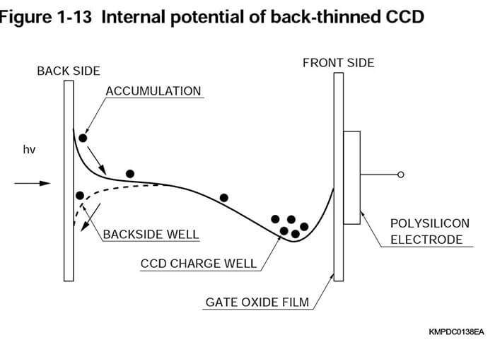
Back-thinned CCDs must be fabricated so that a signal charge generated near the light input surface (backside) collects into CCD potential wells formed near the front surface. To achieve this, the substrate must undergo thinning and accumulation pro- cesses. Typically, the substrate is thinned to approximately 20 m thick so that resolution is not impaired when the generated charges diffuse toward the CCD potential wells. The accumula- tion process ensures that an internal electric field is formed from the light input surface (backside) toward the front surface. This prevents a signal charge generated very close to the light input surface from recombining through the interface level formed on the light input surface. A typical potential profile created in this way inside a back-thinned CCD is shown in Figure 1-13.
Soft X-rays, ultraviolet light and electrons are absorbed in very shallow regions a few nanometers to a few micrometers deep from the input surface, and generate a signal charge (elec- trons). Back-thinned CCDs can detect these photons with high efficiency.
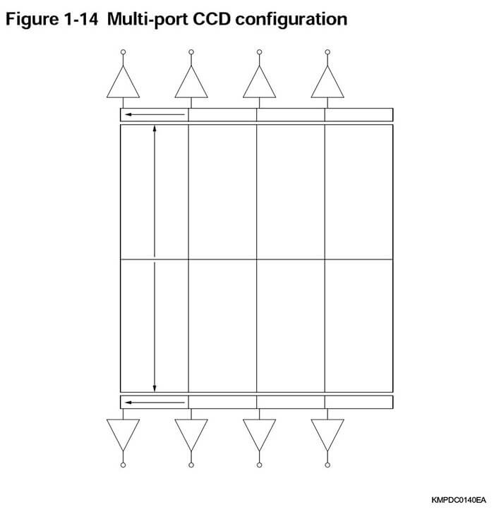
Multi-port CCD
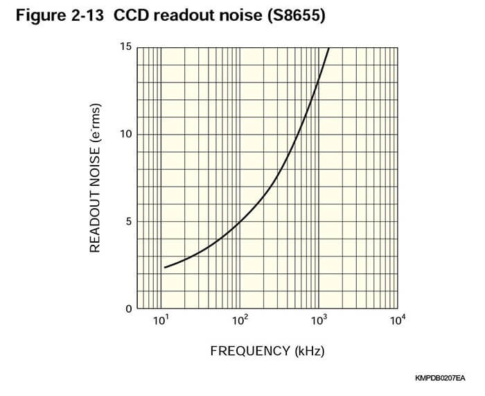
Readout of signals from CCDs with a large number of pixels takes an extremely long time because of limited signal fre- quency. For example, when reading out signals from 1024 × 1024 pixels at a signal frequency of 100 kHz, the readout time will be 10 or more seconds. The signal frequency must be in- creased in order to shorten the readout time. However, the sig- nal frequency and readout noise are a trade-off since increas- ing the signal frequency also increases the readout noise. (Fig- ure 2-13) The CCD frame rate (number of frames acquired per second) is limited by the CCD register transfer frequency and amplifier bandwidth. However, using multiple CCD amplifiers can im- prove the frame rate even if the signal frequency is the same, because parallel readout can be performed as shown in Figure 1-14.
Thermoelectrically cooled CCD
CCD dark current changes with temperature. For example, dark current is usually reduced by one-half for every 5 to 7 °C de- crease in temperature. Cooling a CCD image sensor, along with using the MPP operation, is an effective way to reduce dark current and enhance detection limit.
Cooling a CCD image sensor is very simple with a built-in ther- moelectric cooler. Hamamatsu provides various types of thermoelectrically-cooled CCD image sensors. Cooling tem- perature is determined by heat absorption capacity (Qmax) of the built-in thermoelectric cooler and heat dissipation capacity of the package mounted on the hot side of the thermoelectric cooler. The following thermoelectric cooler parameters differ by product.
Maximum current Imax
Maximum voltage Vmax
Maximum heat absorption Qmax
When using a thermoelectrically cooled device, always operate within the rating values listed in the data sheet to prevent dam- aging the thermoelectric cooler and CCD.
When thermoelectric cooler power consumption is less than 2 or 3 W (watts), the CCD is efficiently cooled by a simple heatsink and natural convection. However, if power consumption is higher than this level, the target convection temperature may be incorrect depending on heat dissipation capacity. This is be- cause the power consumption suddenly increases and the tem- perature on the hot side of the thermoelectric cooler becomes too high. In this case, a larger heatsink, forced air convection cooling or liquid convection cooling is necessary. Thermoelec- tric coolers are designed to cool a CCD image sensor most efficiently when used within 60 % of the maximum current.
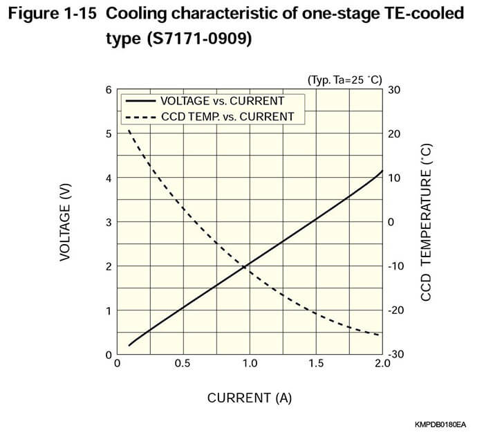
As a rough guide, CCD image sensors are cooled down to the following temperatures when ambient temperature is 25 °C:
One-stage thermoelectrically cooled type : -10 °C
Two-stage thermoelectrically cooled type : -20 to -30 °C
Three-stage thermoelectrically cooled type: -50 to -70 °C
For stable and reliable operation, the thermoelectric cooler cur- rent and heat dissipation condition should be selected accord- ing to surrounding ambient temperature.
1-11 Direct X-ray detection
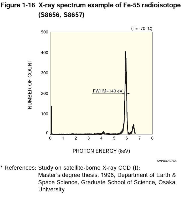
When photons at a certain energy enter a CCD, electron-hole pairs are generated. If photon energy is small like visible light, only one electron-hole pair is generated for each photon. In the vacuum UV and X-ray regions, photon energy is greater than 5 eV so multiple electron-hole pairs are generated by input of one photon. The energy required to produce one electron-hole pair inside silicon is approximately 3.65 eV. For example, an incom- ing photon at 5.9 keV (K of Fe) generates 1620 e- (electrons) in the CCD. This means the CCD can directly detect X-rays, and the number of generated electrons is proportional to the energy of incident photons. The X-ray spectrum can be obtained from just one X-ray photon on the CCD.
Figure 1-16 shows the energy spectrum measured by detecting X-rays incident on a CCD. Spectrum resolution is usually evalu- ated by using FWHM (Full Width at Half Maximum), and the physical limit of energy resolution for Fe-55 is 109 eV. In Hamamatsu CCDs optimized for X-ray detection, the resolution obtained is as high as 140 eV. (Figure 1-16.)
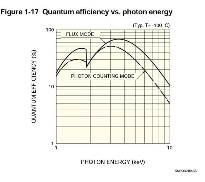
The quantum efficiency the CCD provides in the X-ray region can be determined in either of two modes. One is the photon counting mode in which incident X-ray photons are counted one by one. The other is the flux mode for integrating all pho- tons. The flux mode corresponds to the quantum efficiency re- ferred to when detecting visible light. (Figure 1-17.)
1-12 TDI (Time Delay Integration) operation
In basic CCD operation, a signal charge is accumulated in a potential well separate from other wells. The change is trans- ferred from one well to another towards the output section, like a packet, without being mixed with other individually separated charges. TDI (Time Delay Integration) operation utilizes this CCD charge transfer principle. TDI operation is an effective method for detecting a low-light-level and for imaging a moving or still object from a moving device in which a CCD is installed. Normally, each pixel on a CCD is arrayed in a fixed position, and an image focused on the CCD sensor is detected as a signal charge corresponding to the position of each pixel. This means that the image must stay at the same position on the CCD sensor during the charge integration time. If for some rea- son the image shifts on the CCD sensor, an image smear occurs. When an object is moving at a constant speed, the image al- ways becomes smeary or cannot be recognized at all, though it is possible to capture an image momentarily.
In contrast, TDI operation has the unique feature of being able to capture a clear image of moving objects or if the entire system in which the CCD is installed is moving.
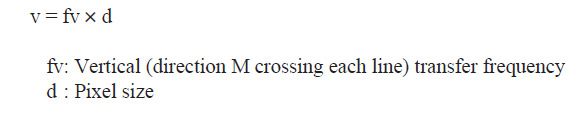
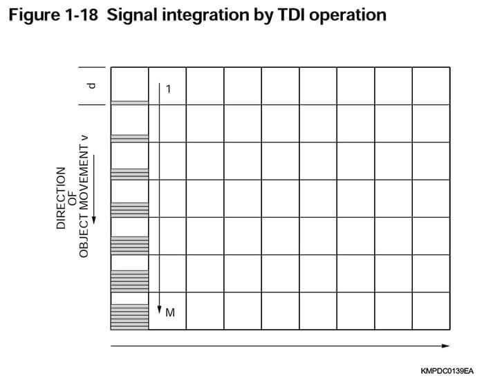
In TDI operation, the FFT-CCD is mainly used. Suppose the constant speed at which an object moves on the CCD active surface is v. The signal charge is integrated at the same position by synchronizing the CCD vertical (direction crossing each line) transfer with fv, because the input corresponding to a certain pixel moves along with the charge transfer.
In Figure 1-18, if the object is moving at a speed v in the direc- tion toward M, then the input to the first row moves to the second row position after a time 1/fv (=d/v). Concurrently with this move- ment, when the first row charge is transferred to the second row, a charge is accumulated by photoelectric conversion in the sec- ond row. When this operation is continuously repeated until reaching the last row M, a signal charge which is M times larger than the normal signal charge is accumulated in this period. Since the signal charge on each row is also sequentially output from the CCD horizontal shift register, a 2-dimensional image can be acquired.
2.Electrical/optical characteristics
2-1 Node sensitivity
Node sensitivity is a parameter that determines the charge-to- voltage conversion gain of an FDA (floating diffusion amplifier). As stated, the FDA converts a signal charge to a voltage according to the relation Q=CV. Thus, the signal charge Q (coulombs) appears at the output source (OS) as the output voltage Vout, as follows:
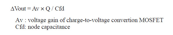
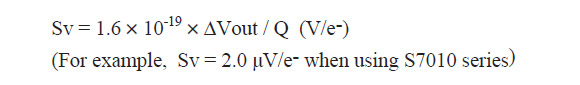
The output amplifier sensitivity Sv is expressed in terms of the ratio of the output voltage  Vout to the signal charge Q, as follows:
Also, the following relation is established for the node capaci- tance Cfd.
2-2 Spectral response
The relation between the incident light wavelength and sensi- tivity (quantum efficiency, etc.) is known as the spectral re- sponse.
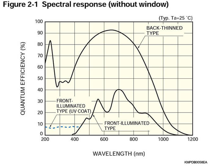
The spectral response is determined on the long wavelength side by the wafer material and on the short wavelength side by the sensor structure. The spectral response of Hamamatsu front-illuminated FFT-CCDs covers from the visible to near in- frared range, with a maximum quantum efficiency of about 40 % at a wavelength between 600 and 700 nm.
Front-illuminated FFT-CCDs require polysilicon gate elec- trodes to be formed on their effective area, making the devices almost insensitive to ultraviolet light at wavelengths shorter than 400 nm.
To make front-illuminated CCDs sensitive to ultraviolet light, the light input faceplate is coated with a Lumogen scintillator that converts ultraviolet into visible light. This method has the disad- vantages of low quantum efficiency and poor long-term stability. In contrast, back-thinned CCDs deliver higher quantum effi- ciency over a spectral range from ultraviolet through near infra- red and have excellent stability during exposure to ultraviolet light.
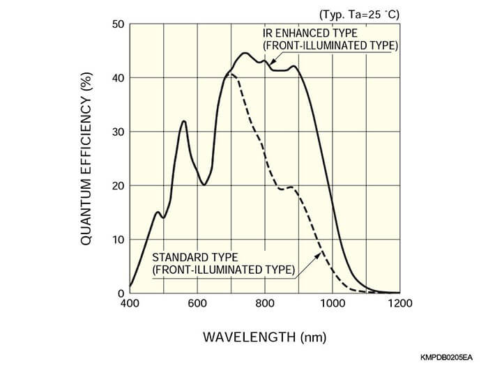
Infrared sensitivity at wavelengths longer than 700 nm depends on the thickness of the photosensitive region, so the quantum efficiency of usual CCDs is not so high in the infrared range. Like CCD image sensor S7847, high quantum efficiency can be achieved even in the infrared range by changing the silicon wafer used to manufacture CCDs.
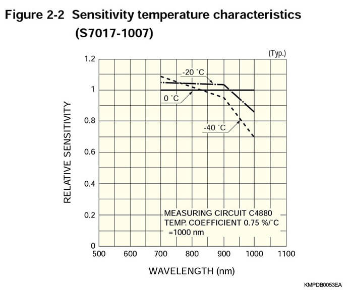
When a CCD is cooled during use, it should be noted that the quantum efficiency drops at wavelengths longer than 800 nm, as shown in Figure 2-2.
hoto Response Non-Uniformity (PRNU)
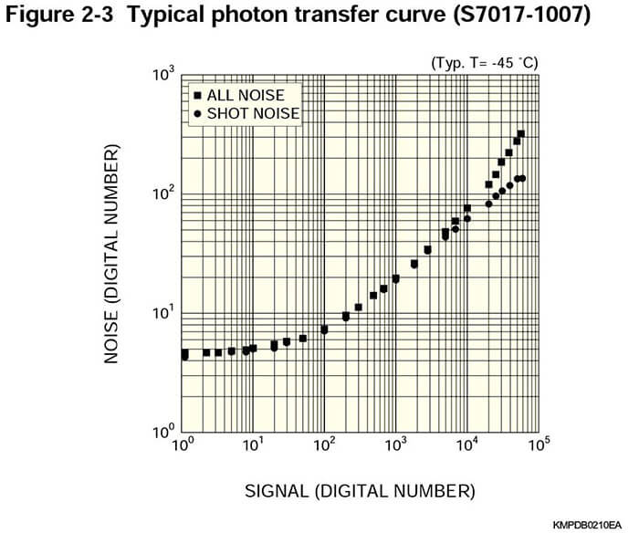
Photo Response Non-Uniformity (PRNU) specifies the varia- tions of response between each pixel, and is viewed as a type of Fixed Pattern Noise (FPN). Photo response non-uniformity be- tween pixels is caused by non-uniformity in quantum efficiency originating from variations in the aperture windows, device structures and wafer processes. The magnitude of photo re- sponse non-uniformity is proportional to the amount of signal. Measuring photo response non-uniformity in CCD area image sensors begins by choosing an area of approximately 50 × 50 pixels from the effective area that are uniformly illuminated. Next, the relationship between the input signal level verses the noise for various exposure. This method is known as “photon transfer”. (Refer to Figure 2-3 plotted where noise is expressed in units of rms.) Photo response non-uniformity (PRNU) is given by:

where Noise is a statistical value (standard deviation of pixel signals), and Signal is the average signal of each pixel. Accord- ingly, when the signal level is low, the PRNU in this measure is influenced by other noise factors. However, when the signal level is sufficient, the PRNU becomes a constant value regard-50 less of the signal level. Therefore, the PRNU specified in the data sheet is measured at a signal level that is about 50 % of the saturation charge (same as Full Well). A typical PRNU for saturation charge (same as Full Well). A typical PRNU for to peak). The data sheet specifies the PRNU in terms of peak to peak value, including the maximum value.
2-4 Full well capacity
The saturation charge for a CCD is equivalent to the number of signal electrons that can be transferred to an adjacent potential well, therefore it is also called the full well capacity (FW). The saturation charge or full well capacity is expressed in terms of the number of electrons (e-), in particular, CCDs intended for scientific application.
The full well capacity for CCDs is determined by the following four factors.
1. Vertical shift register saturation (vertical full well capacity)
2. Horizontal shift register saturation (horizontal full well capacity)
3. Summing well saturation (summing full well capacity)
4. Output section saturation
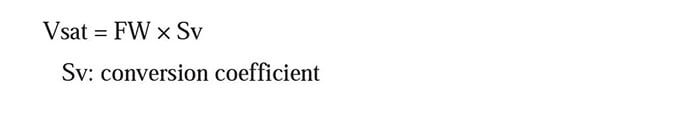
In CCD area image sensor applications, the signal charge of each pixel is output individually, so the saturation is determined by the vertical full well capacity. On the other hand, the horizon- tal full well capacity is designed to saturate at a higher level than to the vertical full well capacity so as to enable line binning (addition of vertical pixel signals). The summing well capacity formed by the summing gate, which is the last clock gate, is designed to be even greater than the horizontal full well capac- ity in order to add the signals from the horizontal shift register (pixel binning). Accordingly, the saturation voltage Vsat of an output signal which is derived as a voltage is generally given by:
2-5. Linearity and linearity residual
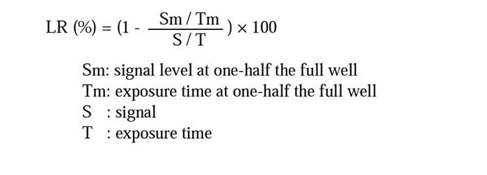
The linearity of CCD input/output characteristics deviates slightly from the ideal line =1. A major cause of this deviation from linearity is related to the output stage. Deviation probably results from capacitive variations caused by the signal charge at the reverse-biased junctions in the FDA. Deviation also re- sults from the subsequent fluctuations in gate voltage on the charge-to-voltage converting MOSFET, causing variations in the transconductance of the MOSFET. To represent the extent of deviation from linearity, the term "Linearity Residual" (LR) is used and defined as follows:
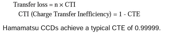
2-6. Charge transfer efficiency (CTE)
Since CCDs are fully charge transfer devices, ideally there is no loss in the transfer process. In practical operation of the device, however, 100 % charge transfer is not attained due to traps resulting from the semiconductor materials and wafer process. Consequently, a tiny amount of charge is not transferred and is left behind.
At Hamamatsu Photonics, Charge Transfer Efficiency (CTE) is defined as the ratio of transferred charge to the accumulated charge per pixel. (In a two-phase clock CCD, in order to transfer charge from one pixel to the next the charge packet must un- dergo two transfers. First, from P1 to P2 within that given pixel, then from P2 to P1 of the next pixel. For CTE measurement, this is specified as one pixel to pixel transfer.)
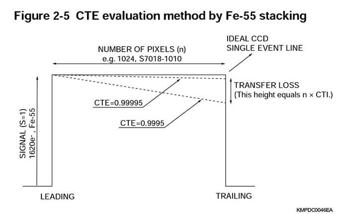
X-ray stimulation is effective in measuring the absolute CTE of a CCD which produces a small charge. This is because X-ray incident on the CCD causes an ideal spot charge in each pixel without using electrical means. In this measurement, the signal of each line in the horizontal direction is stacked (known as horizontal stacking) and plotted. In Figure 2-5, a typical output from the CCD depicts a single pixel event line according to the energy of the X-ray. For ideal CCDs with a CTE equal to 1, the signal height of the leading and trailing edges should be the same. In practice, however, the CTE will not be 1, so signal charge transfer loss occurs at the trailing edge according to the CTE value. If we set the signal charge at the leading edge S as 1, then the loss during transfer is given by:
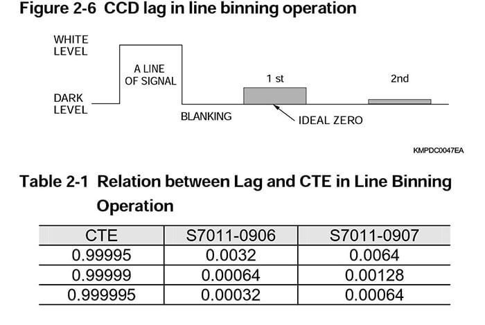
The photodiode signal charge in the photosensitive section of interline CCDs is not completely transferred to the CCD shift register. This may cause a lag as large as several percent. For FFT-CCDs in which the shift register detects light, a lag may occur due to the signal charge which is caught by or released from traps. This results in deterioration in the CTE. Since the two-dimensional operation does not create significant prob- lems with the CTE, let us briefly discuss the lag associated with the CTE, taking line binning as an example.
In line binning, the signal is obtained as a line of signals corre- sponding to the number of horizontal shift register elements. With a CTE of 1 (ideal CCD), no signal charge remains at the subsequent readouts (1st, 2nd, ...) so the signal level returns to the dark level. However, where the CTE is not 1, part of the signal charge stays unread depending on the number of trans- fers, as shown by the shaded area in Figure 2-6.
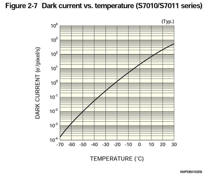
2-7 Dark current
A CCD exhibits a small output even when no incident light is present. This is known as the dark current or dark output. The dark current or output is generally expressed in units of am- peres (A), A/cm2, and volts (V). In CCDs intended for scientific applications, however, the dark current is represented in units of e-/pixel/second; i.e., the number of electrons generated per pixel in unit time.
Three major causes of dark current are as follows:
(1) Thermal generation and diffusion in neutral region
(2) Thermal generation in depletion region
(3) Thermal generation due to surface state at Si-SiO2 interface
Of these three causes, item 3 is predominant in creating dark current.
Since either case is associated with heat or temperature, the dark current has a strong correlation with temperature. This cor- relation can be accurately approximated by using the equation for intrinsic carrier density.
MPP (multi pinned phase) operation is commonly used to re-duce the effect of the interface state and the resuoperation. It is also important to decrease temperature in the ltant dark cur-rent. The dark current can be significantly lowered by this MPP CCD because the dark current doubles for every 5 to 7 °C in- crease in temperature. In view of the above, cooling the CCD in MPP mode is very effective in scientific applications where reduced the dark cur- rent is essential.
MPP operation is also referred to as inverted operation. Pinning is a condition which results in very low dark current. For pinning to occur, the gate voltage is made increasingly more negative. At a certain (negative) gate voltage, the valence band at the Si/ SiO2 interface reaches the potential of the valance band in the bulk semiconductor. If the substrate is grounded, the holes from the channel stop region “pin” the valence band to ground and no additional change in channel potential will occur. The volt- age at which this occurs is called the pinning gate voltage (Fig- ure 2-8). This is implemented by setting all MOS gates, which constitute the CCD electrodes, to the inverted state. This inver- sion causes the conduction properties of the semiconductor to charge from P-type semiconductor to N-type semiconductor, or vice-versa.
In a two-phase CCD, a potential difference is preset by means of ion implantation or other techniques between the collecting and the barrier phases. This means the CCD still provides the potential well even when all the gates are set to the same volt- age. MPP operation is then performed by applying a bias so all phases of the CCD are set to the inverted state.
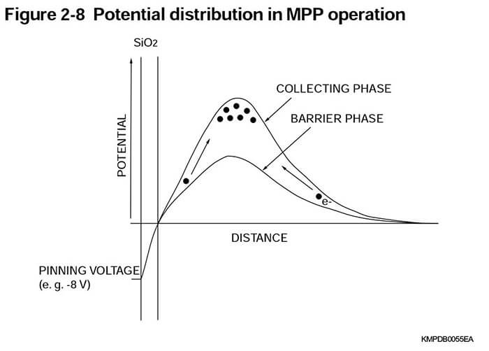
As shown in the potential distribution in Figure 2-8, both the collecting and barrier phases are pinned in the inverted state. In the pinning state, the CCD surface is inverted by holes supplied from the channel stop region. The potential at Si-SiO2 interface is pinned and fixed at the same potential as the substrate, even if a further negative voltage is applied.
In this state while inverted by holes, thermally generated elec- trons at Si-SiO2 interface can be dramatically suppressed, thus achieving a very low dark current level.
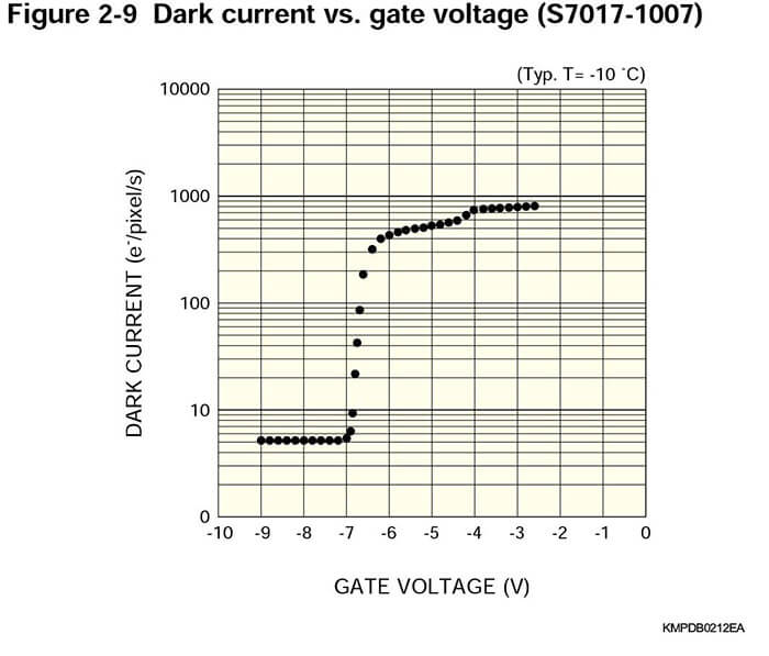
In MPP operation, it is important to apply an optimum pinning voltage since this greatly affects the dark current characteristics. As Figure 2-9 shows, the dark output cannot be reduced to a minimum level at a voltage higher than the optimum pinning voltage (approx. -7 V in the figure) because the inverted layer is not fully formed by holes.
If the negative bias is increased in excess of the optimum pin- ning voltage, an excessively high clock amplitude is required, and spurious charges may increase dark current. It is therefore recommended that the gate voltage be adjusted near the volt- age specified in the data sheet for maximum performance with a minimum dark current.
2-8.Noise
There are numerous sources that generate noise in CCDs, in- cluding those originating from extrinsic factors, such as cosmic rays. These can be categorized into the following four factors when considering only intrinsic noise in CCD elements:
1. Fixed pattern noise (Nf)
Fixed pattern noise of CCD is the variation in photo-response between neighboring pixels. This variation is caused by a small difference in the sensitivity between each pixel. This sensitivity difference results mainly from variations in the quantum effi- ciency among pixels caused by non-uniformities in the aperture area and film thickness that arise during CCD fabrication. When the signal is large, the fixed pattern noise is proportional to the exposure level (number of signal electrons). A fixed pattern noise of Nf=0 is used if considering the noise of one pixel.
2. Shot noise (Ns)
Shot noise is the noise associated with the statistical changes in the number of photons incident on CCD. Other detectors as well as CCDs are affected by shot noise. Shot noise is given as follows according to the Poisson distribution.
Ns=√S
Here, Ns is the shot noise and S is the signal, both expressed in electrons (e-).
For example, if CCD receives photons that generate a signal of 10,000 e- inside the CCD, then the shot noise will be 100 e-rms.
3. Dark shot noise (Nd)
Dark current is affected by shot noise. Since both dark current and photo-response signals are governed by the same physi-cal characteristics, dark shot noise is proportional to the square root of the number of electrons generated in a dark state. To reduce the effects of dark shot noise, the dark current itself must be minimized.
The variation of dark current between neighboring pixels is larger than that of sensitivity.
4.Readout noise (Nr)
This is the electrical noise resulting from thermal noise caused by MOSFET devices that make up the CCD output amplifiers and from readout circuit noise. This readout noise (Nr) eventu- ally determines the lower detection limit of the CCD. Readout noise is related to CCD readout operations and is therefore constant independent of the signal quantity, though it is fre-quency dependent. See section 2-11 for more details.
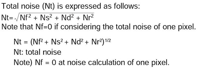
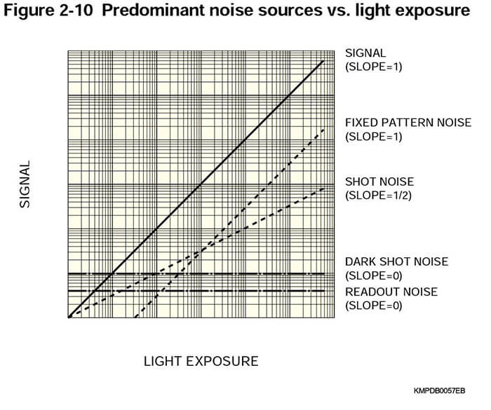
Figure 2-10 shows how these four factors are related to amount of exposure. The dark shot noise resulting from the dark current is always constant regardless of the number of incident photons as long as exposure time is constant. Likewise, the readout noise is independent of the amount of exposure, as it is deter- mined only by the CCD output method. The performance of a CCD can be enhanced up to its detection limit (readout noise) by operating the CCD under conditions where the dark shot noise is reduced below the readout noise. As stated previously, cooling the CCD operated in the MPP mode is most effective in reducing the dark current.
The S/N during operation is determined by the fixed pattern noise at higher exposure levels, and the shot noise at lower exposure levels. The noise factors that affect the detection limit are dark shot noise and readout noise. Since dark shot noise largely depends on the dark current, if sufficiently minimized, readout noise ultimately governs the detection limit or the mini- mum level of the dynamic range discussed in the next section.
2-9 Dynamic range
The term dynamic range refers to the range in which a measur- ing device or detector is capable of accurately measuring the signal. Dynamic range is the ratio of maximum to minimum sig- nal levels (detection limit) that is detected. The dynamic range is the saturation charge (full well capacity) divided by the readout noise. Since the detection limit depends on both dark shot noise and readout noise, the dynamic range varies with operating conditions, such as operating tempera- ture and charge integration time.
The dynamic range is determined by the readout noise under operating conditions where the CCD is cooled adequately so that dark shot noise can be ignored. Therefore the dynamic range listed in the data sheet shows the optimum range for maximum effectiveness. Since the upper detection limit is determined by the full well capacity, the dynamic range (DR) is given by:
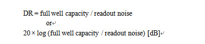
The full well capacity becomes equal to the saturation charge of the vertical shift register. When operated in the line binning or pixel binning, the saturation process differs slightly. It is neces- sary to substitute the horizontal full well for the numerator in order to figure out the dynamic range, depending on the opera- tion method.
Signal-to-noise ratio (SNR) is the signal level divided by the read out noise. Since the total noise is dependent on the photon shot noise, dark shot noise and readout noise, the SNR varies with operating conditions, such as CCD temperature and inte- gration time. When the CCD is at room temperature and in com- plete darkness, the detection limit is mostly affected by the dark shot noise.
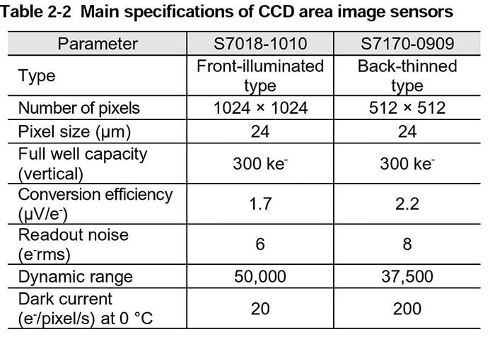
2-10 Resolution
The modulation transfer function (MTF) is commonly used to quantify the resolution of an image sensor that reproduces the contrast at a certain spatial frequency of the scene. Since the active area of a CCD consists of discrete pixels, it exhibits a limiting resolution determined by the Nyquist limit based on the discrete sampling theorem. For example, when a black-and- white pattern is viewed with a CCD, the difference between the black and white signal levels decreases as the pattern be- comes finer, finally reaching the point at which the pattern can- not be resolved. The ideal MTF is expressed as follows:

where f and fn are the spatial frequency and spatial Nyquist frequency of the scene, respectively.
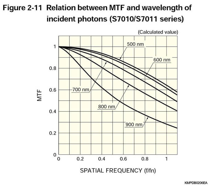
However, because of the difficulty of creating an optical sine wave, a test pattern that provides a square wave is generally used. In this case, the spatial frequency response is called the contrast transfer function (CTF) to distinguish it from the MTF. (Note that the CTF can be converted into the MTF by means of a Fourier transform.)
Actual CCD resolution is determined by the extent of diffusion occurring before the signal charge collects inside the silicon. When the incident photons are absorbed within the depletion layer, the generated charge does not diffuse and is collected by the corresponding pixels. Consequently, the resolution does not deteriorate. In other words, the resolution depends on the depth in the silicon where the incident photons are absorbed. The longer the incident photon wavelength, the more the reso- lution deteriorates.
2-11 Frequency characteristics of noise
When dark current and spurious charges are sufficiently small, the readout noise determines the number of noise electrons generating in a CCD. The readout noise is also determined by the thermal noise of the MOSFET comprising the FDA in the readout section. The MOSFET thermal noise can be expressed by white noise component and 1/f noise component. The factor that determines white noise component is the MOSFET mutual conductance (gm). Simply increasing the gm does not result in a noise decrease, because the effects of 1/f noise also appear. To achieve low noise, both white noise and 1/f noise must be re- duced. In MOSFET device used with CCDs for scientific appli- cations, the corner frequency of 1/f noise is reduced to as low as a few kilohertz.
The MOSFET thermal noise also depends greatly on the bias condition. To use a CCD with the readout noise specified in the data sheet, the bias operation must comply with the recom- mended operating conditions. Even when the recommended operating conditions are maintained, the signal processing cir- cuit still has a great effect on CCD readout noise. Since a CDS circuit is usually used for CCD signal processing, CCD readout noise can be reduced by optimizing the transfer function be- tween the CDS circuit and the LPF (Low Pass Filter) installed in the previous stage of the CDS circuit. If the effect of the 1/f noise corner frequency can be reduced versus CCD readout fre- quency, then the output noise of the CCD system, including the signal processing circuit, will be determined by the white noise and noise bandwidth. Consequently, CCD readout noise de- pends on the readout signal frequency. The readout signal fre- quency should be less than 100 kHz to deliver the readout noise of the few electrons (e-rms) required for scientific applica- tions. If the signal frequency becomes higher, the readout noise abruptly increases.
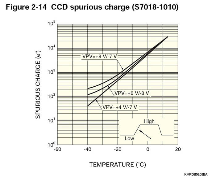
2-12 Spurious charge
Spurious charges are likely generated when a CCD is oper- ated in MPP mode (inverted state of MOS). In MPP mode op- eration, the vertical clock is set to Low. During this period, the region under the gate of each pixel is in an inverted state by holes. In this inverted state, holes moves from the channel stop region to a point under the gate, and the surface potential in that region is pinned at bulk potential. At the same time, some holes are trapped along the oxide interface and their phase becomes a non-inverted state when the clock is set to High level. The holes that have been trapped have high en- ergy after released, and generate a spurious charge which is then collected in the potential well. When the CCD signal is read out, this spurious charge should be added to the dark current listed in the data sheet since it is not included in data sheet spec.
The spurious charge is improved by decreasing the leading edge slope of the clock or reducing the voltage difference between High and Low clock levels. When a CCD is cooled to a sufficiently low temperature so the signal level approaches readout noise level, the clock adjustment must be determined while taking the spurious charge into account.
2-13 Cosmetics
The term cosmetics indicates the specifications and number of CCD blemishes or defects. CCD blemishes are classified into “white spots” that appear white in a dark image and “black spots” that appear black when light is incident on CCD. These white and black spots are also referred to as point defects or pixel defects.
White spots are usually caused by lattice defects in the sub- strate material, metal impurities, or pattern failures from me- chanical damage or dust contamination during wafer process. A process called “gettering” is used to reduce white spots. It is difficult to completely eliminate white spots even by gettering, and white spots stand out a great deal in CCDs with a larger active area and smaller pixels. Black spots, on the other hand are mainly caused by irregular reflection on the CCD surface due to dust deposits during wafer process or to partial defects of the insulation film on the CCD surface. The CCD surface and window faceplate must be kept clean in order to minimize black spots.
Hamamatsu defines white and black spot criteria and inspects every CCD for these spots. Defect definitions are as follows:
(Detect definition may generally differ between manufactures, so keep this point in mind when comparing specifications.)
1. Point defect
White spot
Pixels that generate dark current in excess of 3 % of the full well (FW) capacity after charge integration for one second at a CCD cooling temperature of 0 °C.
Black spot
Pixels that indicate an output of less than one-half the average signal value when CCD is illuminated with uniform light that is 50 to 100 % of the full well (FW) capacity level. At Hamamatsu, CCD is tested illuminating with uniform light that is 50 % of the FW capacity level.
Defects including white and black spots are referred to as point defects.
2. Cluster defect
A defect consisting of 2 to 9 continuous white or black spots is called a “cluster defect” and is viewed as different from a point defect. Cluster defects appear vertically in most cases, but may appear as a two-dimensional cluster if originating from black spots of back-thinned CCDs or front-illuminated CCDs coupled to an FOS.
3. Column defect
A defect consisting of 10 or more continuous white or black spots (defect larger than cluster defect) is called a “column de-fect”, and is viewed as different from a cluster defect. Like the cluster defect, the column defect also appears vertically in most cases, but may appear as a two-dimensional cluster if originat- ing from black spots of back-thinned CCDs or front-illuminated CCDs coupled to an FOS.
Front-illuminated CCDs with a small active area, for example Hamamatsu S7010/S7011/S7015 series CCD image sensors, have no defects. When CCDs are coupled to a FOP or FOS, defects may occur due to other factors not originating in the CCDs, so the shape and quantity of defects will differ from those occurring in CCDs only.
3.Peripheral circuits
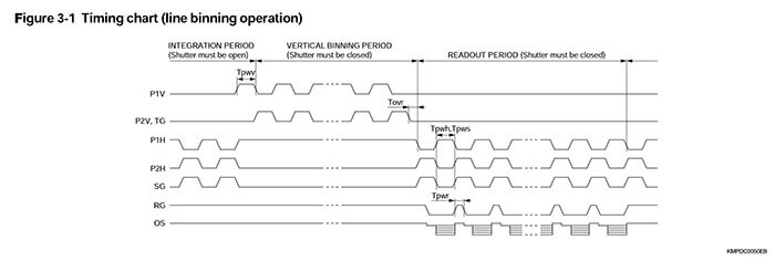
3-1 Timing
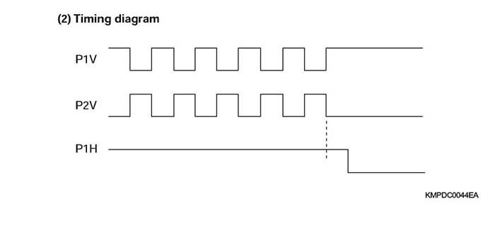
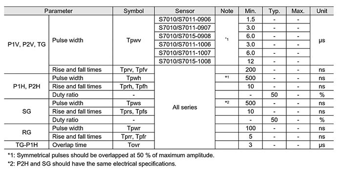
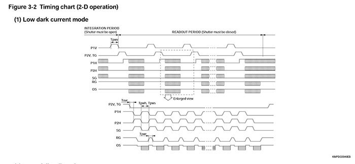
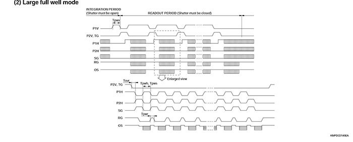
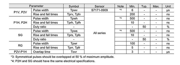
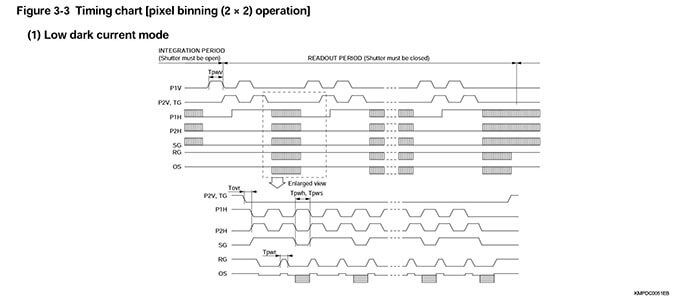
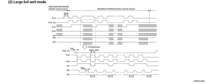
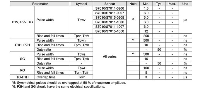
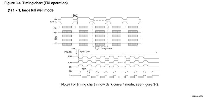
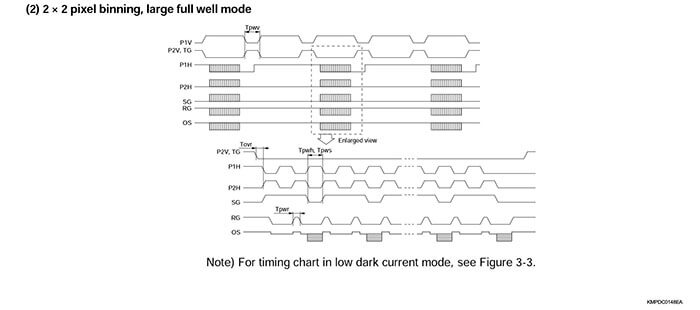
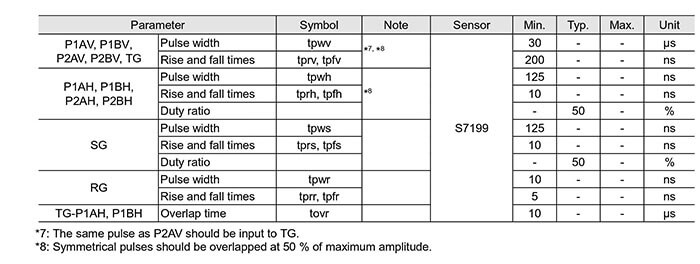
Operating a CCD image sensor requires 7 types of signals: a two-phase clock pulse (P1V, P2V) for the vertical shift register, a transfer gate pulse (TG), another two-phase clock pulse (P1H, P2H) for the horizontal shift register, a summing gate pulse (SG) and a reset pulse (RG). TG is provided by dividing the last P2V electrode. The TG pulse should have the same timing as P2V. A separate drive is recommended, though operation is also possible by shorting the TG and P2V terminals.
Figures 3-1 to 3-4 show the timing diagram for operating a CCD image sensor. As described in "1-5 Binning of signal charge", FFT-CCD image sensors can be operated in anyone of the 4 modes: line binning, two-dimensional operation, pixel binning mode or TDI operation. The desired mode can be chosen by simply adjusting the timing of each signal.
(1) Line binning
Pixel signals in the vertical register are first transferred (binned) in the horizontal register. This permits the signal charges to be added to the horizontal shift register, and then all the horizontal signal charges are transferred. As with two-dimensional opera- tion, the summing gate pulse (SG) should be as exactly the same as the clock pulse (P2H) for the horizontal shift register.
(2) Two-dimensional operation
This operation transfers all the horizontal pixel signals each time one pixel of the signal charge is transferred in the vertical direction. When signal charge transfer in the vertical direction is complete, a frame transfer has been performed. At this point, the summing gate pulse (SG) should be set exactly as the clock pulse (P2H) for the horizontal shift register.
(3) Pixel binning
The pixel signals are transferred in some units. All the horizon- tal signal charges are then transferred. At this point, by halting the summing gate pulse (SG) for a period equal to the number of bits required for summing, the signal charges are added to the summing well. Note: Line binning and pixel binning can be performed at the same time.
(4) TDI operation
As explained in section 1-12, TDI operation allows imaging of a moving object. To do this, the CCD vertical transfer clock must be synchronized with the speed that the object moves along the CCD surface.
Notes:
1. Dark current listed in the data sheet is measured in MPP operation mode with a low level clock applied to P1V and P2V. Dark current will be larger when used in other opera- tion modes.
2. When a signal charge is read out, the dark currents in the following periods are also included.
• Integration time
• Readout time (vertical transfer period)
• Readout time (horizontal transfer period)
In “large full well mode” shown in Figure 3-2, the dark cur- rent generated in the vertical transfer period becomes larger than that in “low dark current mode”.
3. The full well capacity of the vertical register listed in the data sheet becomes equal to the value in “large full well mode” shown in Figure 3-2. The full well capacity in “low dark cur- rent mode” is about one-half that in “large full well mode”.
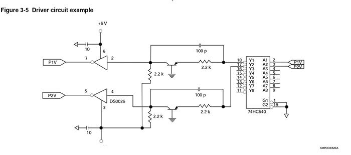
3-2 Driver circuit
An H-level pulse with +6 V amplitude and a L-level pulse with -8 V amplitude are required to drive a CCD image sensor. These pulses are used to operate a vertical shift register having an input capacitance of several hundred to several thousand picofarads. These pulses are also used in operating the hori- zontal shift register. Use of an MOS driver capable of driving capacitive loads at high speeds is preferred. TTL or CMOS logic ICs are used in making the driver circuit compatible with other peripheral logic circuits that employ use TTL or CMOS. Since these ICs operate from +5 V supply, a voltage level converter is required for connection to the MOS driver. Figure 3-5 shows an example of CCD driver circuits.
3-3 Output circuit
An on-chip MOS-FET for charge-to-voltage conversion, called a floating diffusion amplifier, is incorporated into the output stage of a CCD image sensor. This MOS-FET is of the source follower type, having its source terminal used as an external terminal (OS) that allows connection of an external load resistance (RL) to prevent additional overheating. The drain terminal is also used as an external terminal (OD). This MOS-FET is designed to minimize 1/f noise even at room temperatures. Readout noise is therefore considerably reduced. A typical output circuit is shown in Figure 3-6.
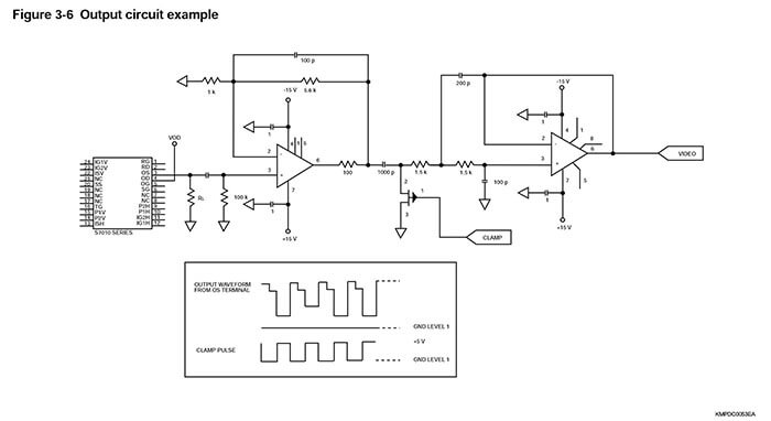
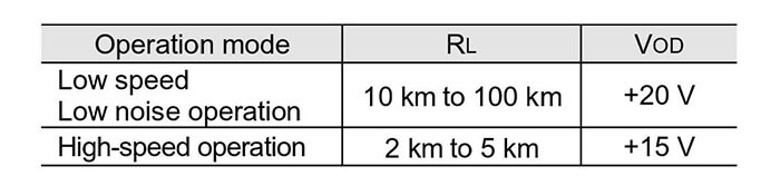
The load resistance (RL) and the MOS-FET drain voltage (VOD) should be set depending on the type of CCD image sensor operation: low-speed and low-noise operation or high-speed operation.
A DC offset voltage (caused by resetting the charge detection node to the reset drain voltage VRD=12 V) is included in the sensor output. AC coupling is used for connection to the pream- plifier. Since AC coupling is accompanied by variations in the overall reference level depending on light intensity, a clamping circuit is placed in the latter stage to fix the reference level at GND level. This circuit is used as part of the CDS circuit de- scribed in section 3-4.
3-4 Signal processing circuit
Major sources of noise from a CCD image sensor include KTC and 1/f noise. KTC noise is generally referred to as reset noise and inevitably occurs in CCD image sensors and similar de- vices that perform discharging by a charge-to-voltage converter (reset operation). This noise is proportional to the square root of the capacitance of the charge-to-voltage converter and makes up a large percentage of the total noise of a CCD image sensor. The 1/f noise is generated by the MOS-FET.
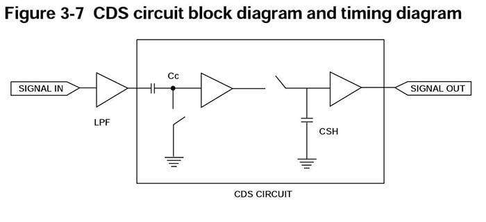
These noise sources can be removed by using a CDS (corre- lated double sampling) circuit. Figure 3-7 shows a block dia- gram of a CDS circuit along with the timing diagram. The CDS circuit consists of a lowpass filter (LPF), a clamping circuit, and a sample and hold circuit. Its operation is simple. The level im- mediately after reset (feedthrough level) is clamped at a certain voltage, then the signal level is sampled. This eliminates the KTC noise and 1/f noise, thus leaving only the intrinsic noise charge which generally attains a level of several 10 e-rms or several e-rms.
4.Precautions for use
4-1 Electrostatic and surge measures
CCD area image sensors may be damaged or deteriorate if subjected to static electricity and voltage surges. Take the fol- lowing precautions to avoid trouble.
(1) Handling precautions
When taking a CCD image sensor out of the package, al- ways do so in locations where anti-electrostatic measures are provided. For example, lay a grounded conductive sheet (1  to 100 ) on the work bench or work floor. When handling CCD sensors, wear anti-static clothing, gloves and shoes, and a ground wrist strap. (The wrist strap should have a high resistance of about 1 on the side closer to the body and be grounded properly. Not using the wrist strap is very hazardous because you may sustain an electrical shock if electric leakage occurs.)
Always ground the soldering iron so no leakage voltage is applied.
Do not bring a charged object (insulator material such as plastics and vinyl, VDT for PC) close to CCD image sensors. (CCD image sensors might be electrically charged just by being brought close to a charged object, leading to electro- static damage.)
(2) Precautions during use
Measurement devices used with CCD image sensors must be properly grounded so no surges are applied by a leak- age voltage. Do not to allow a voltage higher than the maxi- mum rating (from measurement device, etc.) to be applied to CCD image sensors. (This tends to occur during ON/OFF switching of power sources, so use caution.) If there is the possibility of a voltage surge, insert a filter (made up of a resistor or capacitor) to protect the CCD image sensors.
When installing the CCD image sensor into the socket, be extremely careful to avoid reverse insertion, wrong insertion and terminal pin shorting.
Do not attach or detach any power supply line or output line connector during operation.
(3) Precautions for carrying or shipping
When carrying or reshipping a CCD image sensor, place it on a conductive mat by inserting the lead pins into the mat (for shorting lead pins) and then put it in a conductive case. The PC board to mount the CCD image sensor should also be put in a conductive case. Avoid using plastic or styrofoam packages as they may generate static electricity by vibration during shipping, causing breakdown or deterioration.
(4) Precautions for storage
When storing a CCD image sensor, place it on a conductive mat by inserting the lead pins into the mat (for shorting lead pins) and then put it in a conductive case. The PC board to mount the CCD image sensor should also be put in a con- ductive case. Avoid using plastic or styrofoam packages as they may generate static electricity by vibration during ship-ping, causing breakdown or deterioration. Avoid placing equipment that may generate high voltage or high magnetic fields near image sensors.
It is not always necessary to provide all the electrostatic and surge measures stated above. Implement these measures according to the amount of damage that occurs.
4-2 Windowless type
Windowless CCD image sensors are available for detection of vacuum UV or soft X-rays. Extreme care must be taken when handling these sensors to avoid damage to the CCD chip and bonding wires. Do not use these sensors in environments where moisture condensation may occur (including cases where the sensors are thermoelectrically cooled). Please note that windowless image sensors are not covered by Hamamatsu’s standard warranty.
4-3 Faceplate (window)
Contamination or scratches on the faceplate (window) may de- grade uniformity. Before using the image sensor, the faceplate must be cleaned. Use a soft cloth or cotton swab moistened with organic solvent, such as alcohol, to wipe off the faceplate. Do not rub the faceplate with a dry cloth or cotton swabs as these may generate static electricity.
Be careful not to drop the image sensor or to apply strong fric- tion on the faceplate as this may cause scratches on the face- plate. Extreme care should be taken when handling the image sensor.
4-4 Installation
When installing an image sensor into the socket on the circuit board, note the correct pin positions and package orientation. Take care to avoid generating static electricity during installing. Once the image sensor has been installed correctly, turn on the power supply.
References
1) J. R. Janesick, "Scientific Charge-Coupled Devices", SPIE PRESS, 2001
2) A. S. Grove, Physics and Technology of Semiconductor Devices, John Wiley and Sons
3) S. B. Howell, Handbook of CCD Astronomy, CAMBRIDGE UNIVERSITY PRESS
4) M. Muramatsu et al, "Greater than 90% QE in Visible Spectrum Perceptible from UV to near IR Hamamatsu Thinned Back-Illuminated CCD", SPIE 3019 (1997) 2
5) K. Miyaguchi et al, "CCD developed for scientific applica- tion by Hamamatsu", NIM A436 (1999) 24
6) Image sensor selection guide (Hamamatsu Photonics)
檔案下載