- HOME
- 產品介紹
- 半導體事業部
- Hamamatsu Photonics
- Image Sensor
- Image Sensor
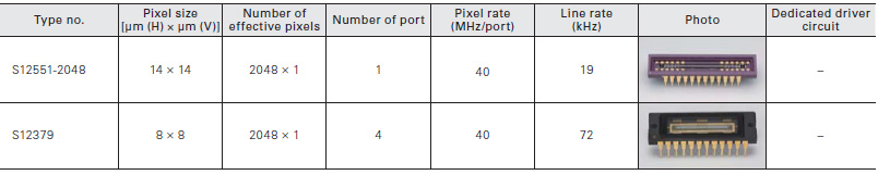
Image Sensor
![]() +886-2-8772-8910
+886-2-8772-8910

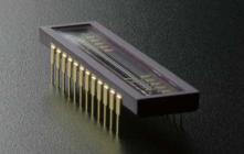
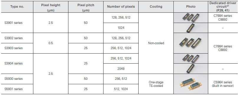
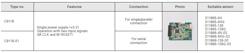
Area image sensors
Linear image sensors
Photodiode arrays with amplifier

Distance image sensors

Image sensors for near infrared region

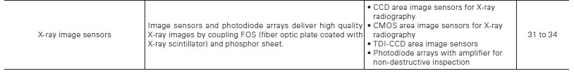
X-ray image sensors
X-ray flat panel sensors

Related products for image sensors
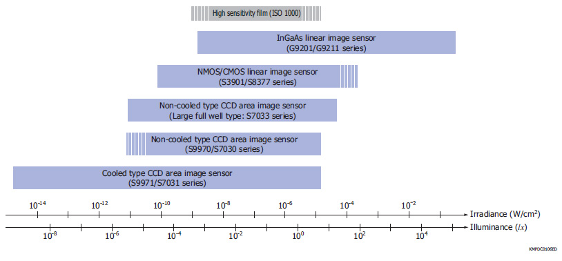
Example of detectable light level
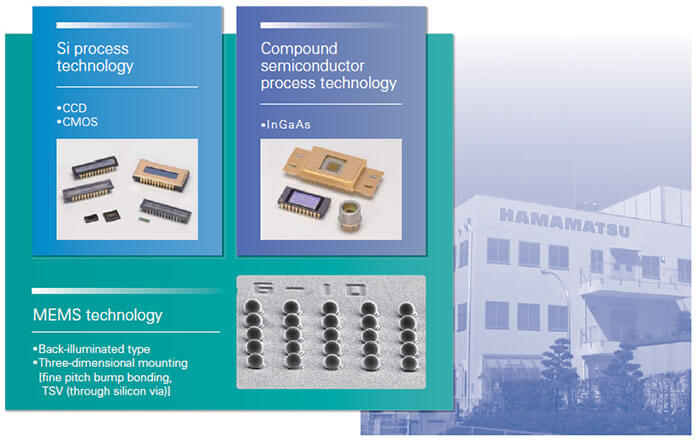
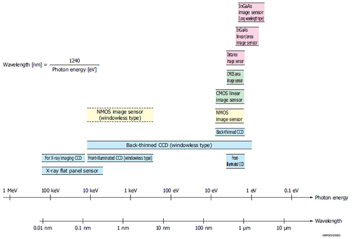
Hamamatsu Photonics uses its original silicon/compound semiconductor process technology to manufacture image sensors that cover a wide energy and spectral range from 2.6 μm near infrared region to visible, UV, vacuum UV (VUV), soft X-ray, and even hard X-ray region. In addition, we also provide module products designed to work as driver circuits for various image sensors.
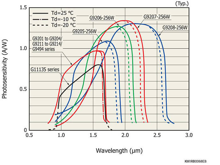
Spectral response
Example of detectable energy level and spectral response range
Note) If using an NMOS image sensor (windowless type) for X-ray direct detection, please consult our sales of fi ce regarding usage conditions.
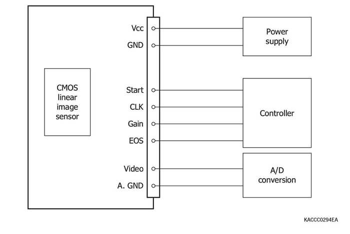
CMOS technology
Hamamatsu produces CMOS image sensors that use its uniquely developed analog CMOS technology at their cores for applications mainly aimed at measuring equipment such as analytical instruments and medical equipment. With analog and digital features that meet market needs built into the same chip as the sensor, systems can be designed with high performance, multi-functionality, and low cost.
• Supports photosensitive areas of various shapes (silicon/compound semiconductor, one- and two-dimensional array, large area)
• Highly functional (high-speed, partial readout, built-in A/D converter, global shutter, etc.)
• Customization for specific applicationss
Example of high functionality based on CMOS technology
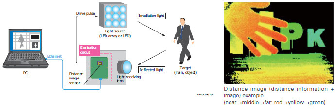
Distance image sensor
This image sensor can detect distance information for the target object using the TOF (time-of-flight) method. A distance measurement system can be configured by combining a pulse-modulated light source and a signal processing section.
Example of distance measurement diagram
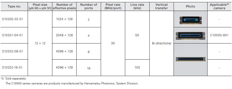
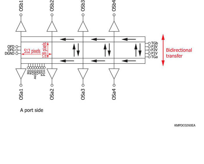
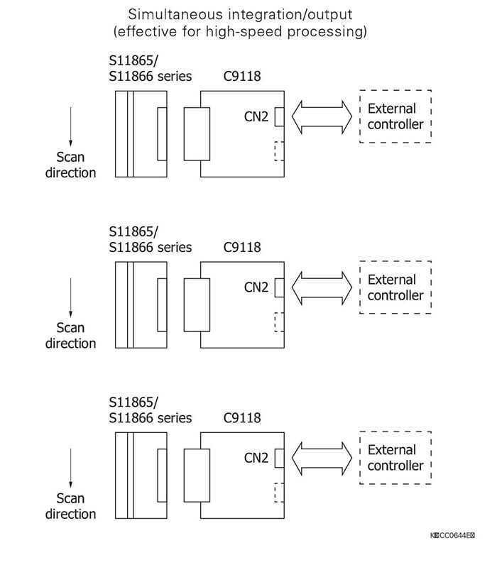
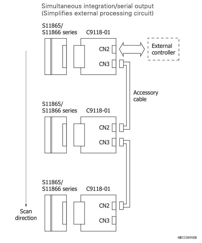
2-port parallel output type image sensor
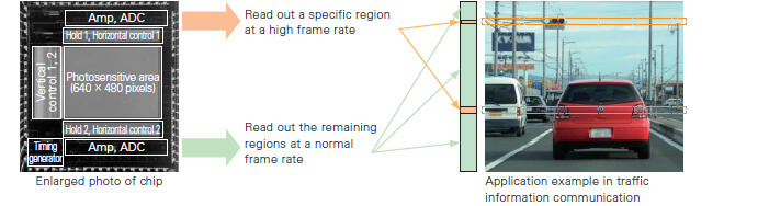
It is possible to create highly functional CMOS image sensors for various applications by using CMOS technology. Here we introduce a 2-port parallel output type as an example. As shown in the figure, a readout circuit can be incorporated on the top and bottom of the photosensitive area, and each circuit can be operated independently. A video line for each circuit is connected to each pixel, and the data of any pixel can be read out from either circuit. It is also possible to read out a specific region at a high frame rate with port 1 and read out the remaining regions at a normal frame rate with port 2.
2-port parallel output type image senso
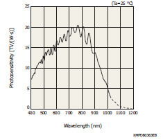
Near infrared-enhanced CMOS area image sensor
Our unique photosensitive area technology provides high sensitivity in the near infrared region.
Hybrid technology (Three-dimensional mounting)
Back-thinned technology
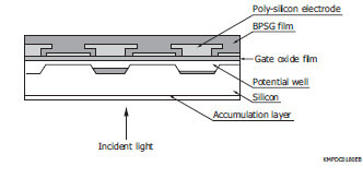
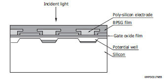
In general, CCDs are designed to receive light from the front side where circuit patterns are formed. This type of CCD is called the front-illuminated CCD. The light input surface of front-illuminated CCDs is formed on the front surface of the silicon substrate where a BPSG film, poly-silicon electrodes, and gate oxide film are deposited. Light entering the front surface is largely reflected away and absorbed by those components. The quantum efficiency is therefore limited to approx. 40% at the highest in the visible region, and there is no sensitivity in the ultraviolet region.
Back-thinned CCDs were developed to solve such problems. Back-thinned CCDs also have a BPSG film, poly-silicon electrodes, and gate oxide film on the surface of the silicon substrate, but they receive light from the backside of the silicon substrate. Because of this structure, back-thinned CCDs deliver high quantum efficiency over a wide spectral range. Besides having high sensitivity and low noise which are the intrinsic features of CCDs, back-thinned CCDs are also sensitive to electron beams, soft X-rays, ultraviolet, visible, and near infrared region.
Schematic of CCDs
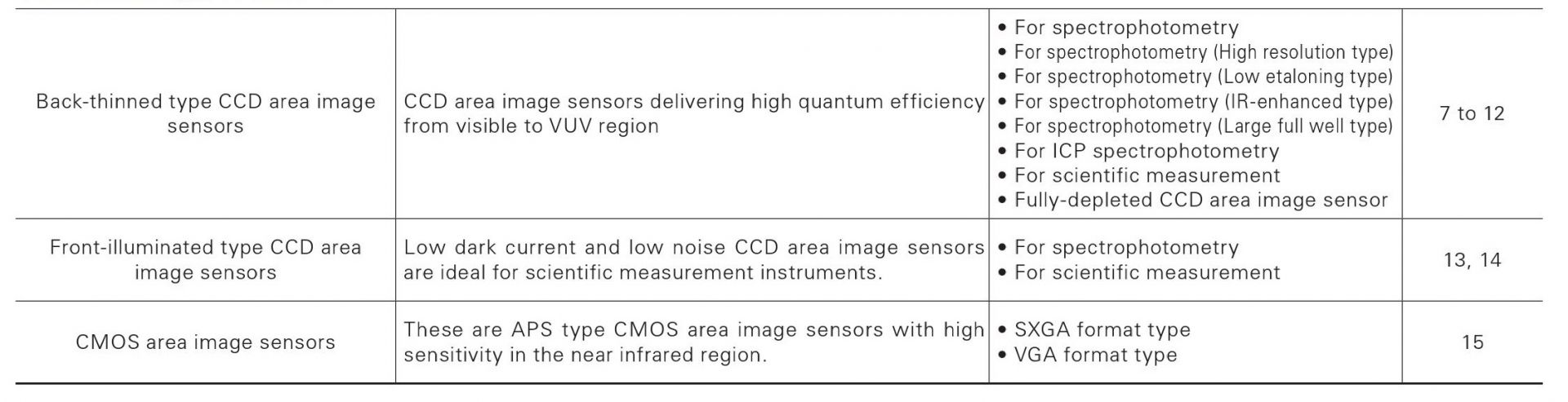
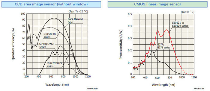
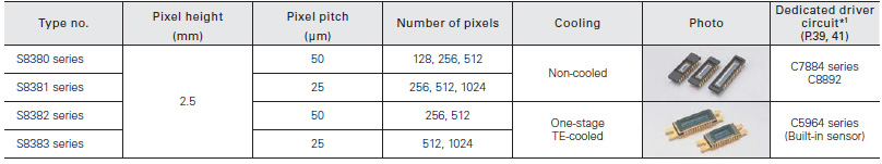
Hamamatsu CCD area image sensors have extremely low noise and can acquire image signals with high S/N. Hamamatsu CCD area image sensors use an FFT- CCD that achieves a 100% fill factor and collects light with zero loss, making them ideal for high precision measurement such as spectrophotometry. These CCD area image sensors are available in a front-illuminated type or a back-thinned type. The front-illuminated type detects light from the front side where circuit patterns are formed, while the back- thinned type detects light from the rear of the Si substrate. Both types are available in various pixel sizes and formats allowing you to select the device that best meets your applications. The rear of the back-thinned type is thinned to form an ideal photosensitive surface delivering higher quantum efficiency over a wide spectral range.
Back-thinned type CCD area image sensors deliver high quan- tum efficiency (90% or more at the peak wavelength) and have great stability for UV region. Moreover these also feature low noise and are therefore ideal for low-light-level detection.
For spectrophotometry
Achieving high quantum efficiency (at peak 90% min.) and ideal for high accuracy spectrophotometry
For spectrophotometry (High resolution type)
CCD area image sensors having superior low noise performance
For spectrophotometry (Low etaloning type)
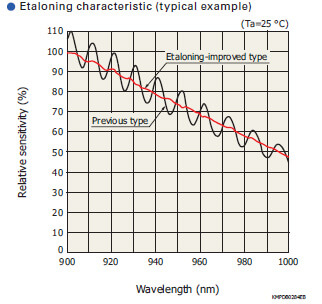
Two types consisting of a high-speed type (S11071 series, S11851-1106) and low noise type (S10420-01 series, S11850-1106) are available with improved etaloning characteristics. The S11850 and S11851-1106 have a thermoelectric cooler within the package to minimize variations in the chip temperature during operation.
Improved etaloning characteristic
Etaloning is an interference phenomenon that occurs when the light incident on a CCD repeatedly reflects between the front and back surfaces of the CCD while being attenuated, and causes alternately high and low sensitivity. When long- wavelength light enters a back-thinned CCD, etaloning oc- curs due to the relationship between the silicon substrate thickness and the absorption length. The S11071/S10420 - 01 series and S11850/S11851-1106 back-thinned CCDs have achieved a significant improvement on etaloning by using a unique structure that is unlikely to cause interference.
For spectrophotometry (IR-enhanced type)
Enhanced near infrared sensitivity: QE=40% (λ=1000 nm)
Enhanced IR sensitivit
These sensors have MEMS structures fabricated by our own unique laser processing technology. These sensors have achieved very high sensitivity in the near infrared region at wavelengths longer than 800 nm. Utilizing high sensitiv- ity characteristic in the near infrared region, these sensors should find applications in Raman spectroscopy.
For spectrophotometry (Large full well type)
Wide dynamic range are achieved.
For ICP spectrophotometry
This CCD area image sensor has a back-thinned structure that enables high sensitivity in the UV to visible region an well as wide dynamic range, low dark current, and an anti-blooming function.
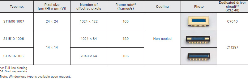
For scientific measurement
Selectable from a line-up covering various types of high performance back-thinned CCD area image sensors such as high-speed readout type and low noise type
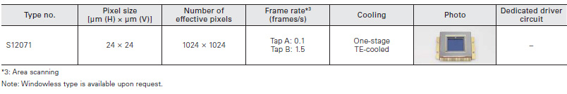
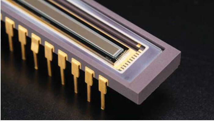
Fully-depleted CCD area image sensor
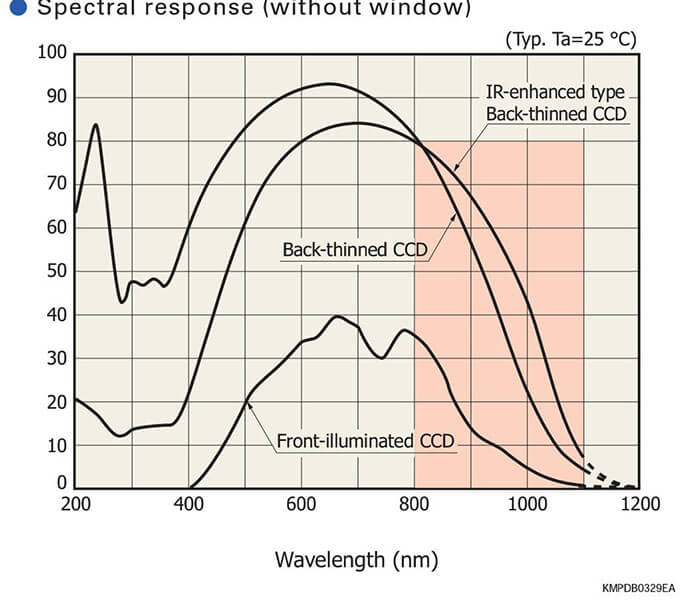
The S10747-0909 is a back-illuminated CCD area image sensor that delivers drastically improved near-infrared sensitivity by the wid- ened depletion layer.
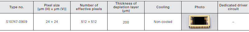
Structure of fully-depleted back-illuminated CCD
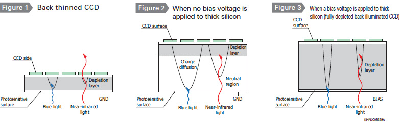
Back-thinned CCDs the silicon substrate is only a few dozen microns thick. This means that near-infrared light is more likely to pass through the substrate (see Figure 1), thus resulting in a loss of quantum efficiency in infrared region. Thickening the silicon substrate increases the quantum efficiency in the near-infrared region but also makes the resolution worse since the generated charges diffuse into the neutral region unless a bias voltage is applied (see Figure 2). Fully- depleted back-illumi- nated CCDs use a thick silicon substrate that has no neutral region when a bias voltage is applied and therefore deliver high quantum efficiency in the near-infrared region while maintaining a good resolution (see Figure 3). One drawback, however, is that the dark current becomes large so that these devices must usually be cooled to about -70 °C during use.
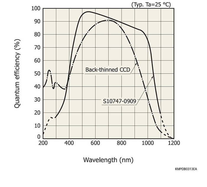
Spectral response (without window)
Front-illuminated type CCD area image sensors are low dark current and low noise CCDs ideal for scientific measurement instruments.
For spectrophotometry
CCD area image sensors specifically designed for spectrophotometry
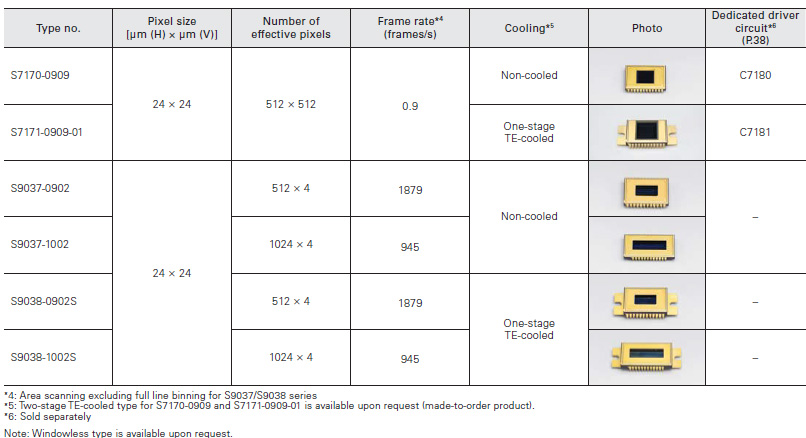
For scientific measurement
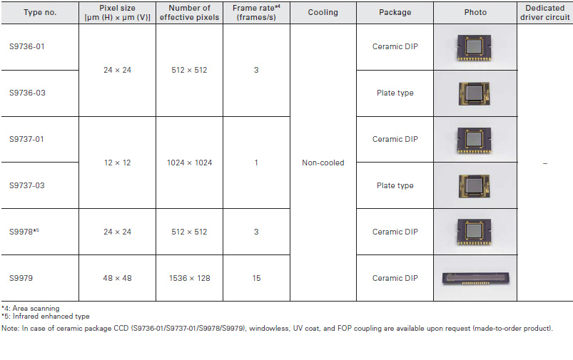
CCD area image sensors that deliver high accuracy measurement. Number of effective pixels of 512 × 512 and 1024 × 1024 are ideal for acquiring two-dimensional imaging.
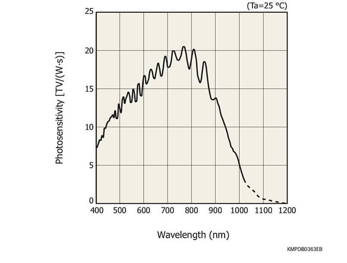
These are APS type CMOS area image sensors with high sensi- tivity in the near infrared region. The S11661 is an SXGA format type, and the S11662 is a VGA format type.
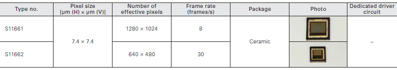
Features of the S11661, S11662
The APS (active pixel sensor) type image sensor consisting of high-sensitivity amplifiers arranged for each pixel achieves high sensitivity in the near infrared region.
The serial/parallel interface allows partial readout setting, global/rolling shutter switching, integration time control, gain and offset control, and so on. It also has a built-in 12-bit A/D converter.
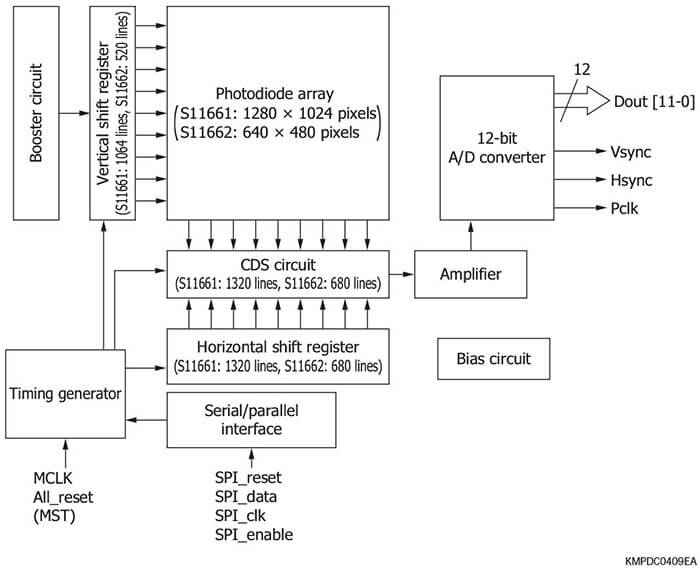
It has a built-in bias circuit and operates on a single 3.3 V power supply input.
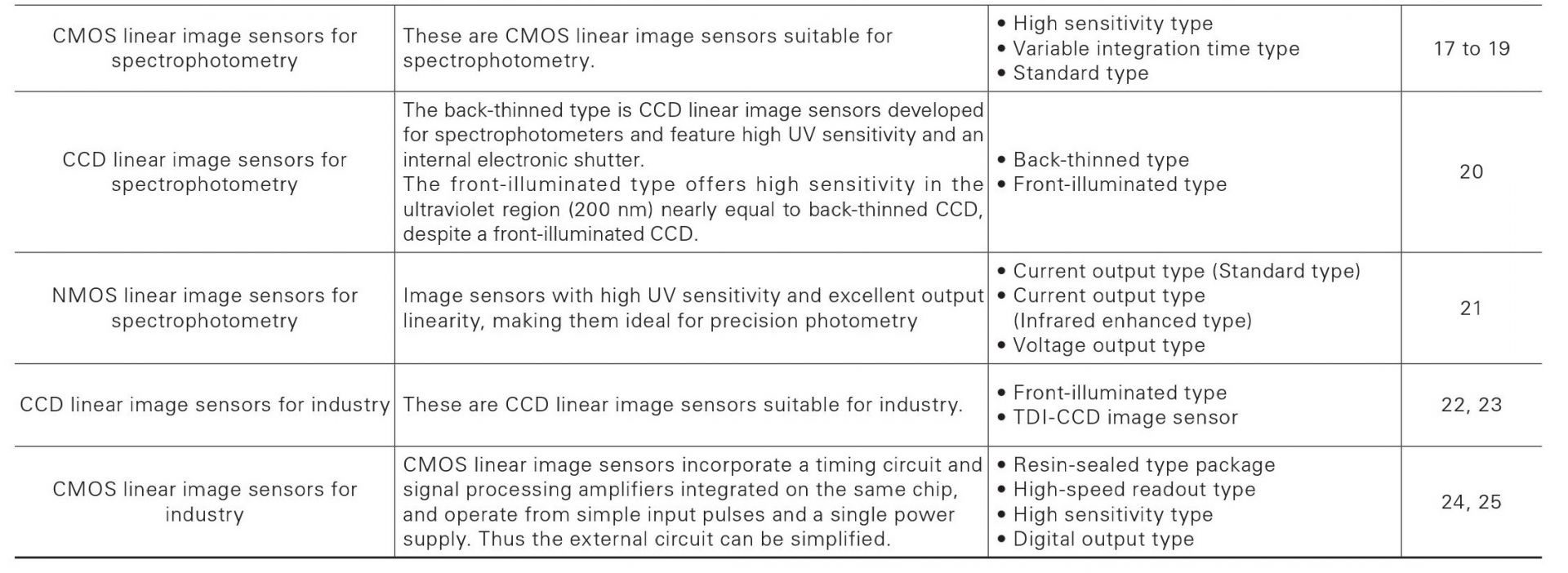
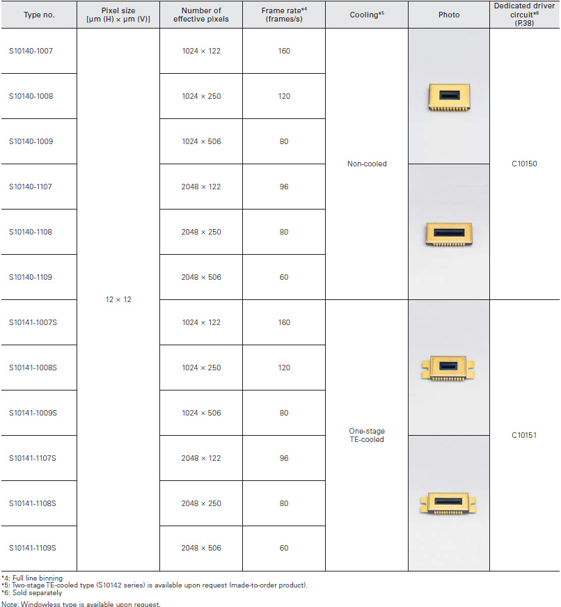
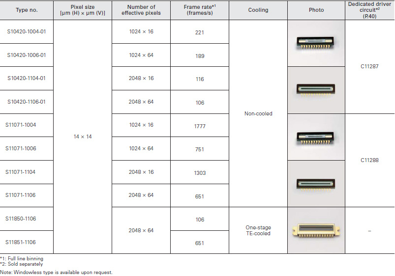
Linear image sensors
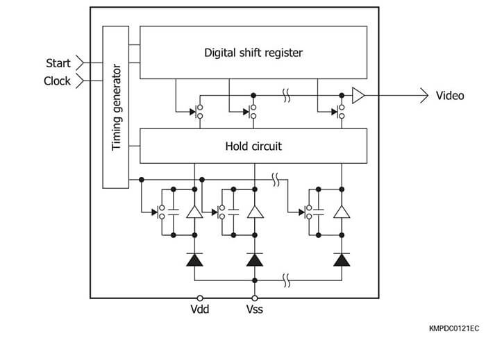
Equivalent circuits
These are CMOS linear image sensors suitable for spectropho- tometry.
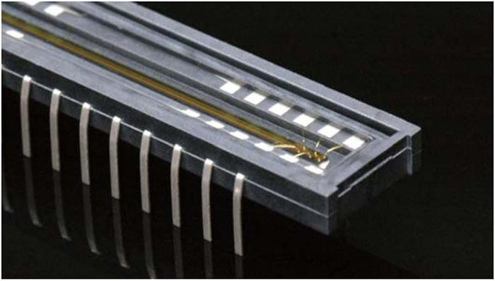
High sensitivity type
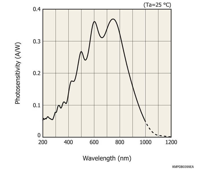
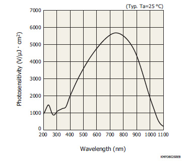
The S11639 is a high sensitivity CMOS linear image sensor using a photosensitive area with vertically long pixels (14 × 200 μm). Other features include high sensitivity and high resistance in the UV region.
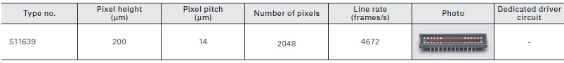
Features of the S11639
For the photosensitive area, a buried photodiode structure is employed to reduce the dark current and shot noise in the dark state. Moreover, the photosensitive area features highly sensitive vertically long pixels but with low image lag, based on our original photosensitive area formation technology. In addition, high sensitivity is also provided for UV light.
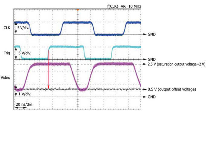
It operates on a single 5 V power supply and two types of external clock pulses. Since the input terminal capacitance of the clock pin is 5 pF, the image sensor can easily be operated with a simple external circuit. The video output is positive polarity. This product generates a readout timing trigger signal, which can be used to perform signal processing.
This APS type image sensor consists of high-sensitivity amplifiers arranged for each pixel. It provides a high charge-to- voltage conversion efficiency of 25 μV/e-, which is higher than that of CCDs.
The image sensor incorporates an electronic shutter function that can be used to control the start timing and length of the integration time in sync with an external clock pulse. The signals of all pixels are transferred to a hold capacity circuit where each pixel is read out one by one.
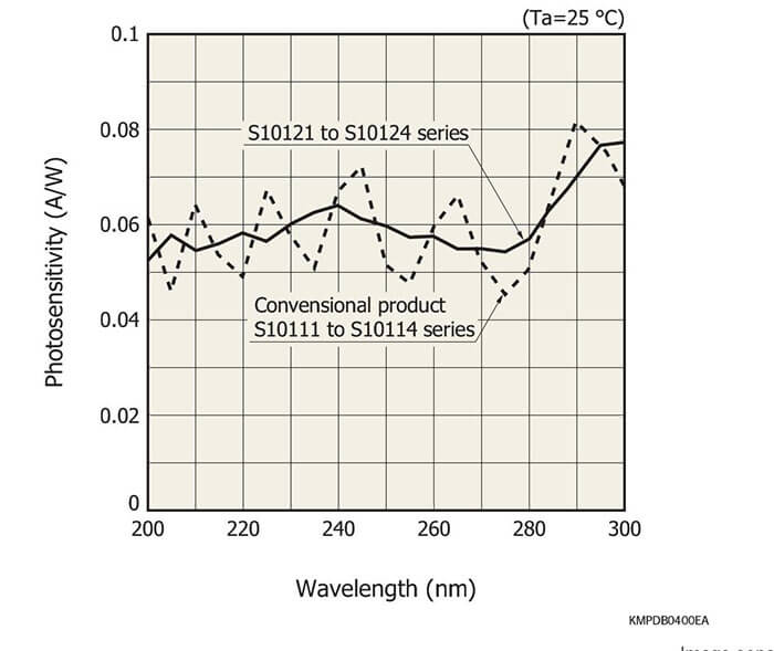
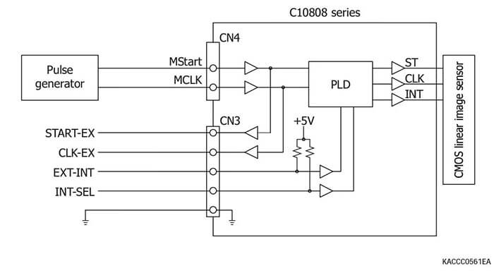
Variable integration time type
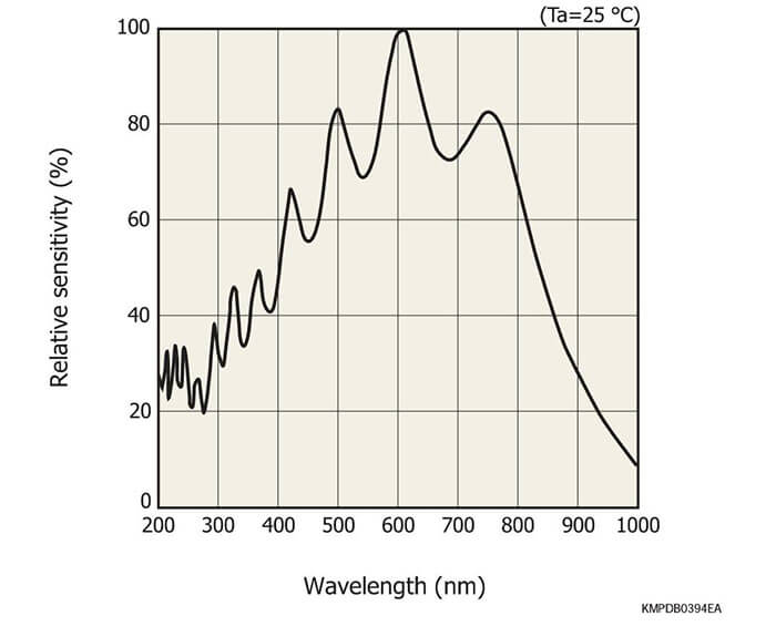
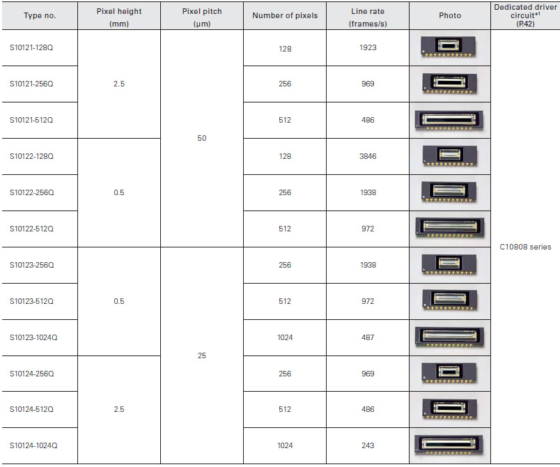
These current output type linear image sensors have a variable integration time function and spectralresponse characteristics with high UV sensitivity. The S10121 to S10124 series also features smoothly varying spectral response characteristics in UV region.
Standard type
CMOS linear image sensors with internal readout circuit
The back-thinned type is CCD linear image sensors developed for spectrophotometers and feature high UV sensitivity and an internal electronic shutter. The front-illuminated type offers high sensitivity in the ultravio- let region (200 nm) nearly equal to back-thinned CCD, despite a front-illuminated CCD.
Back-thinned type
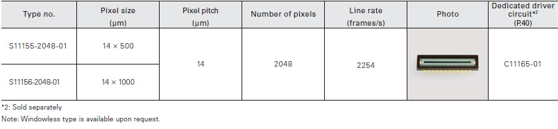
The S11155-2048 and S11156-2048 are back-thinned CCD linear image sensors with an internalelectronic shutter for spectrometers.
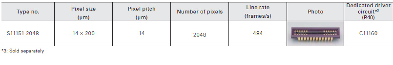
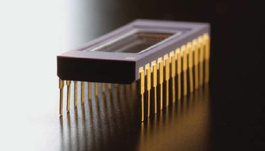
Front-illuminated type
The S11151-2048 is a front-illuminated CCD linear image sensor with high sensitivity and high resistance to UV light.
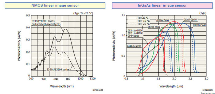
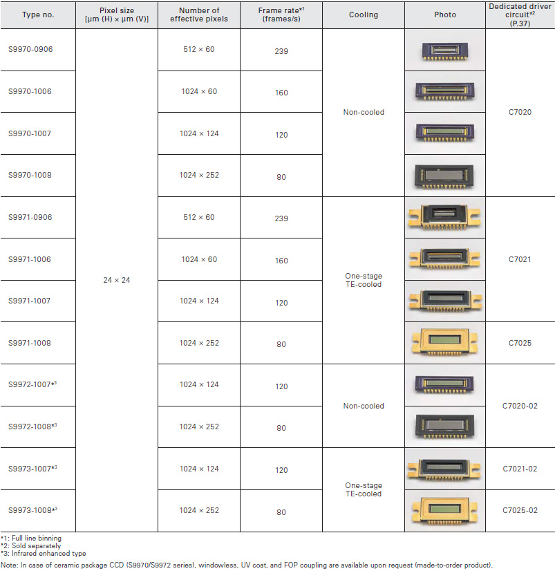
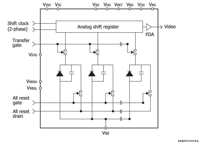
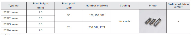
NMOS linear image sensors are self-scanning photodiode arrays de- signed specifically for detectors used in multichannel spectroscopy. These image sensors feature a large photosensitive area, high UV sensitivity and little sensitivity degradation with UV exposure, wide dy- namic range due to low dark current and high saturation charge, supe- rior output linearity and uniformity, and also low power consumption.
Current output type (Standard type)
NMOS linear image sensors offering excellent output linearity and ideal for spectrophotometry
Current output type (Infrared enhanced type)
NMOS linear image sensors having high sensitivity in near infrared region
Voltage output type
These voltage output sensors need only a simple design circuit for read-out compared to the current output type.
These are CCD linear image sensors suitable for industry.
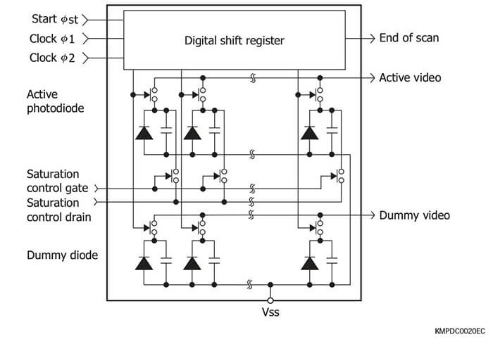
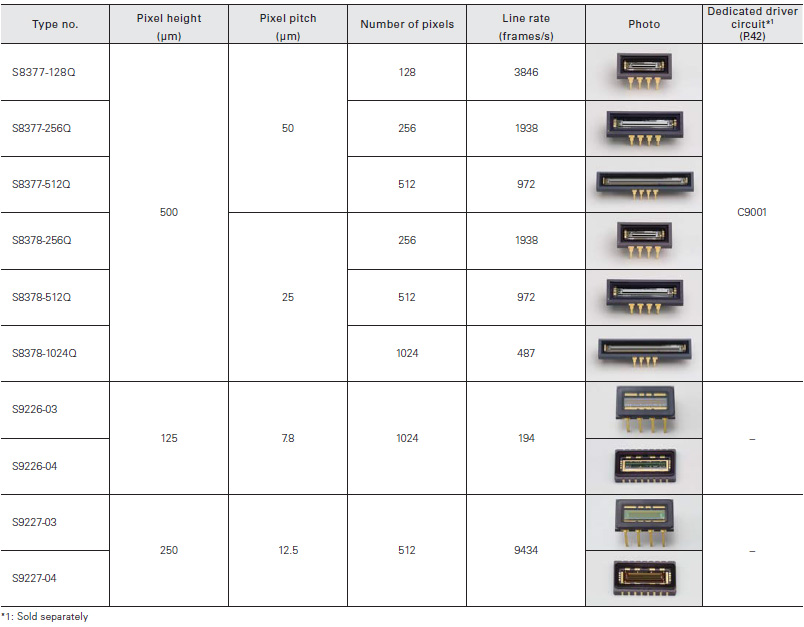
TDI-CCD image sensor
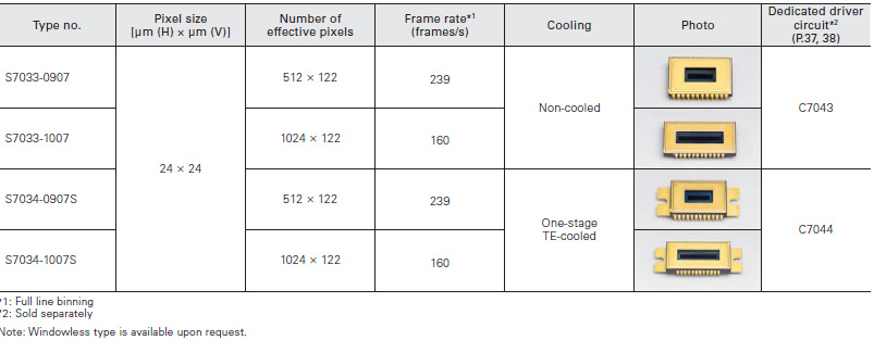
TDI-CCD captures clear, bright images even under low-light-level conditions during high-speed imaging. During TDI mode, the CCD captures an image of a moving object while transferring integrated signal charges synchronously with the object movement. This operation mode drastically boosts sensitivity to high levels even when capturing fast moving objects. Our new TDI-CCD uses a back-thinned structure to achieve even higher quantum efficiency over a wide spectral range from the UV to the near IR region (200 to 1100 nm).
TDI (Time Delay Integration) mode
In FFT- CCD, signal charges in each line are vertically trans- ferred during charge readout. TDI mode synchronizes this vertical transfer timing with the movement timing of the object incident on the CCD, so that signal charges are in- tegrated a number of times equal to the number of vertical stages of the CCD pixels.
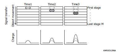
The back-thinned (back- illuminated) structure ensures higher sensitivity than front-illuminated types in the UV through the near IR region (200 to 1100 nm).
Using multiple amplifiers (multiple output ports) permits paral- lel image readout at a fast line rate.
Front-illuminated type
These are front-illuminated type CCD linear image sensors with high-speed line rate designed for applications such as sorting machine.
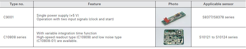
CMOS linear image sensors incorporate a timing circuit and sig- nal processing amplifiers integrated on the same chip, and op- erate from simple input pulses and a single power supply. Thus the external circuit can be simplified.
Resin-sealed type package
These are CMOS linear image sensors of small and surface mounted type suited for mass production.
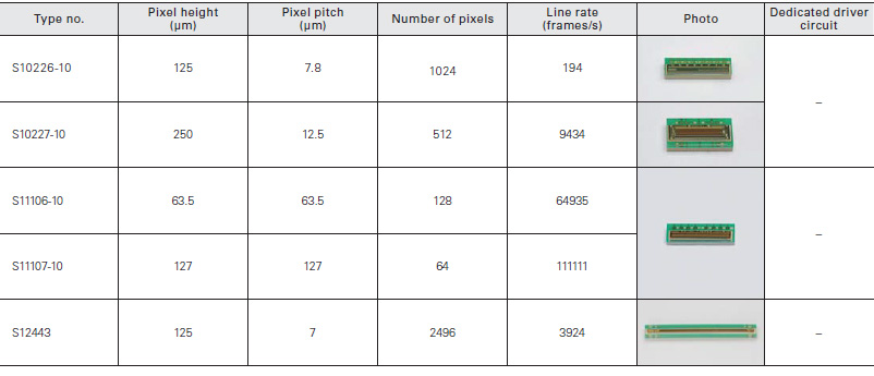
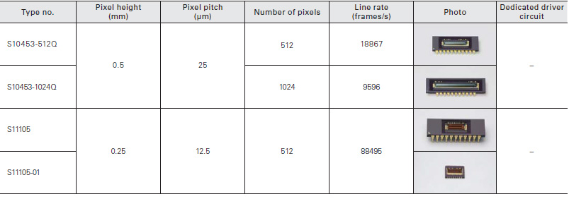
High-speed readout type
These are CMOS linear image sensors with simultaneous charge integration and variable integration time function that allow high- speed readout: 10 MHz (S10453-512Q/-1024Q), 50 MHz (S11105/-01).
High sensitivity type
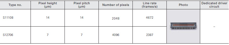
CMOS linear image sensors that achieve high sensitivity by adding an amplifier to each pixel.
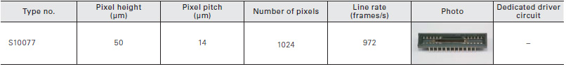
Digital output type
CMOS linear image sensor with internal 8-bit/10-bit AD converter
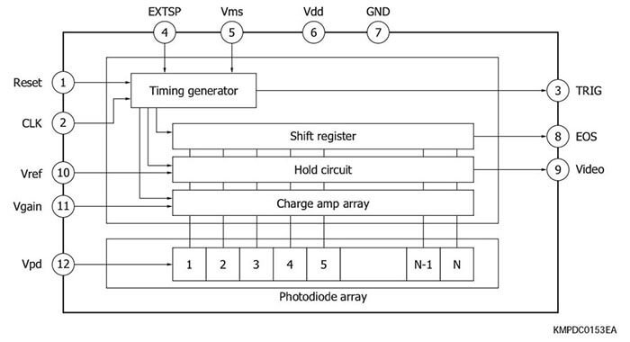
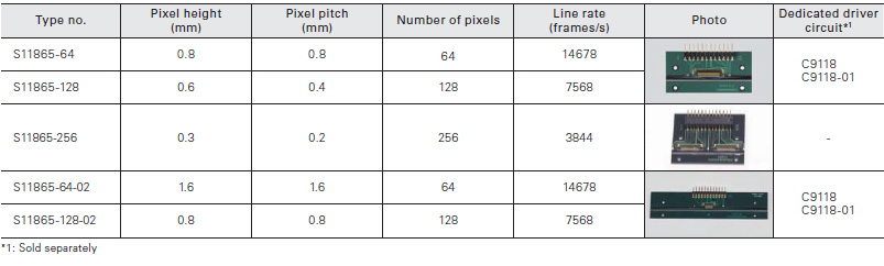
Photodiode arrays with amplifier
Photodiode arrays with amplifier are a type of CMOS image sensor designed mainly for long area detection systems using an equal- magnification optical system. This sensor has two chips consisting of a photodiode array chip for light detection and a CMOS chip for signal processing and readout. A long, narrow image sensor can be configured by arranging multiple arrays in a row.
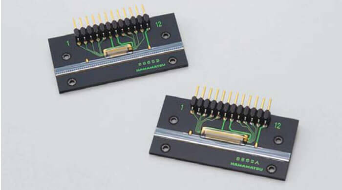
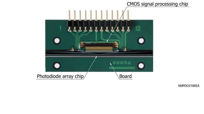
Long and narrow area type
Linear image sensors designed for industrial inspection
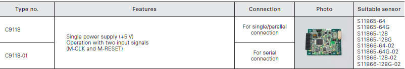
Driver circuits for photodiode arrays with amplifier
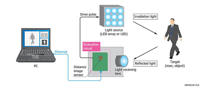
These distance image sensors are designed to measure the dis- tance to an object by TOF method. When used in combination with a pulse modulated light source, these sensors output phase difference information on the timing that the light is emitted and received. The sensor output signals are arithmetically processed by an external signal processing circuit or a PC to obtain distance data.

Example of distance measurement diagram
Distance linear image sensor
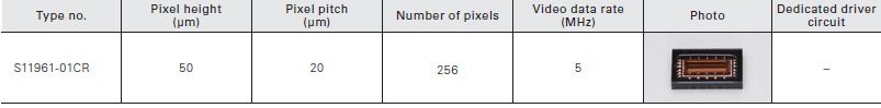
Distance linear image sensor
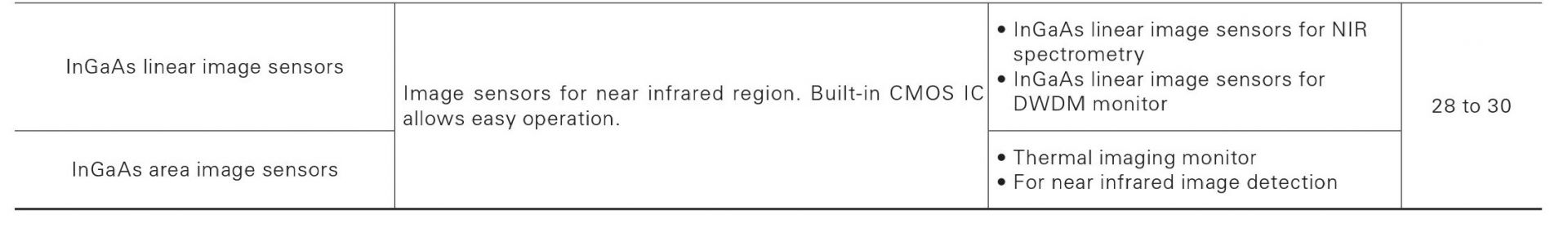
In Ga As image sensors are designed for a wide range of applications in the near infrared region. Built- in CMOS IC readout circuit allows easy signal processing. These image sensors use a charge amplifier mode that provides a large output signal by integrating the charge, making them ideal for low-light-level detection.
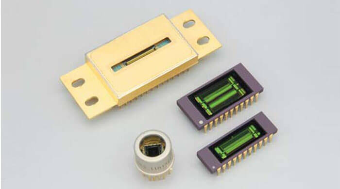
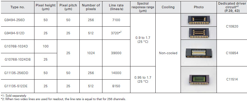
InGaAs linear image sensors for DWDM monitor
These InGaAs image sensors are developed for DWDM (Dense Wavelength Division Multiplexing) monitors in optical fiber commu- nications. 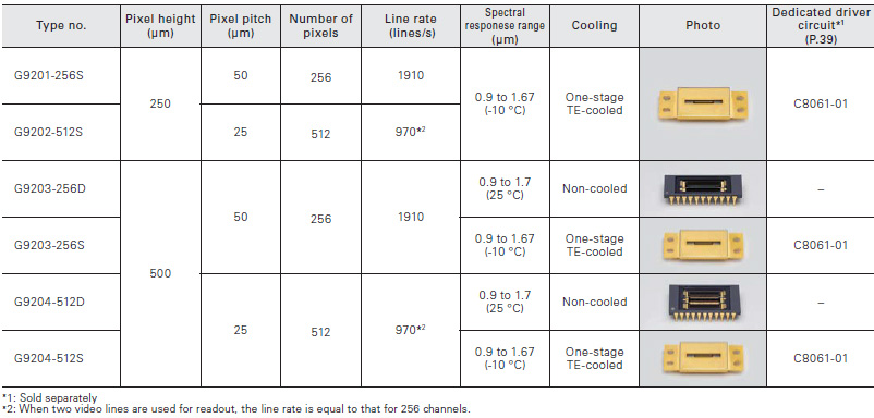
InGaAs linear image sensors for NIR spectrometry
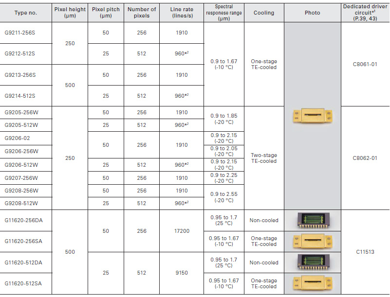
InGaAs linear image sensors are ideal for near-infrared spectrophotometry. The G11135/G11620 series employ a back-illuminated structure and so enable a single video line.
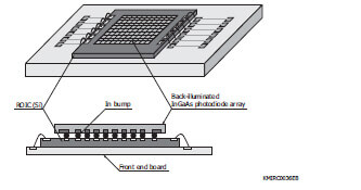
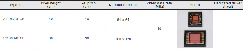
InGaAs area image sensor
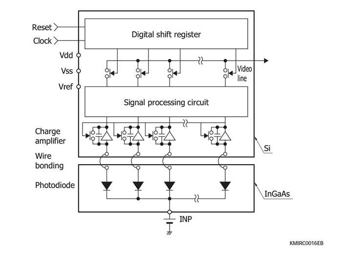
The InGaAs area image sensors have a hybrid structure consisting of a CMOS readout circuit (ROIC: readout integrated circuit) and back-illuminated InGaAs photodiodes.
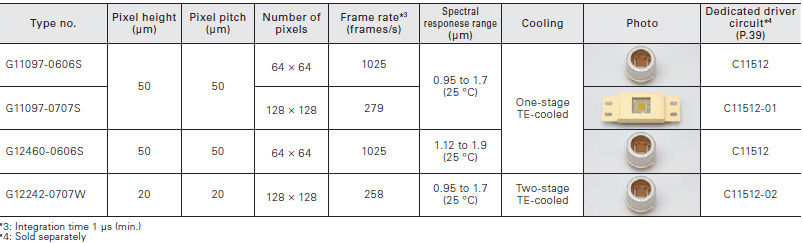
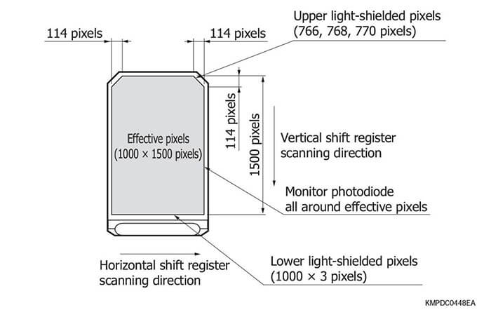
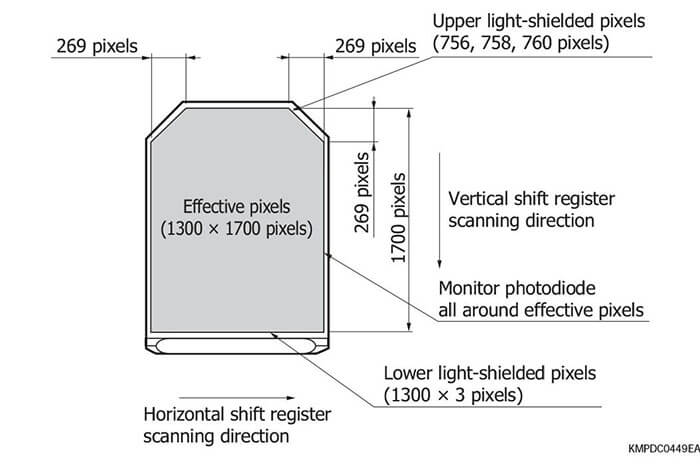
Block diagram (G11097-0606S/-0707S, G12460-0606S)
A sequence of operation of the readout circuit is de- scribed below.
In the readout circuit, the charge amplifier output voltage is sampled and held simultaneously at all pixels during the integration time determined by the low period of the master start pulse (MSP) which is as a frame scan signal. Then the pixels are scanned and their video signals are output.
Pixel scanning starts from the starting point at the upper left in the right figure. The vertical shift register scans from top to bottom in the right figure while sequentially selecting each row.
For each pixel on the selected row, the following opera- tions are per-formed:For each pixel on the selected row, the following opera- tions are per-formed:
●Transfers the sampled and held optical signal informa- tion to the signal processing circuit as a signal voltage.
●Resets the amplifier in each pixel after having trans-ferred the signal voltage and transfers the reset volt-age to the signal processing circuit.
© The signal processing circuit samples and holds the signal voltage º and reset voltage º.
® The horizontal shift register scans from left to right in the right figure, and the voltage difference between and º is calculated in the offset compensation circuit. This eliminates the amplifier offset voltage in each pix- el. The voltage difference between º and º is output as the output signal in the form of serial data.
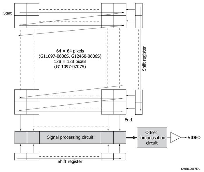
The vertical shift register then selects the next row and repeats the operations from º to ®. After the vertical shift register ad- vances to the 64th row (G11097-0606S, G12460-0606S) or 128th (S11097-0707S), the MSP, which is a frame scan signal, goes low. After that, when the MSP goes high and then low, the reset switches for all pixels are simultaneously released and the next frame integration begins.
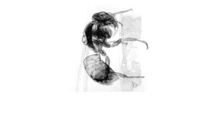
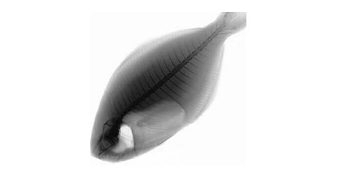
X-ray image sensors
Image sensors and photodiode arrays deliver high quality X-ray images by coupling FOS (fiber optics plate coated with X- ray scintillator) and phosphor sheet.
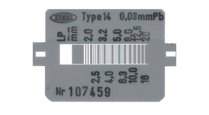
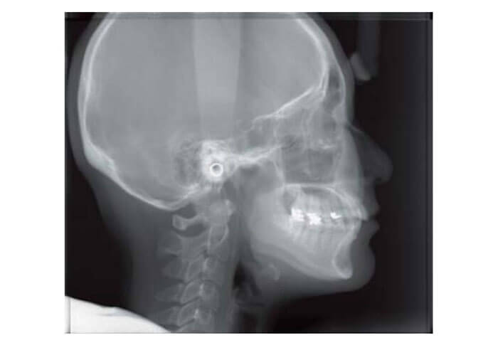
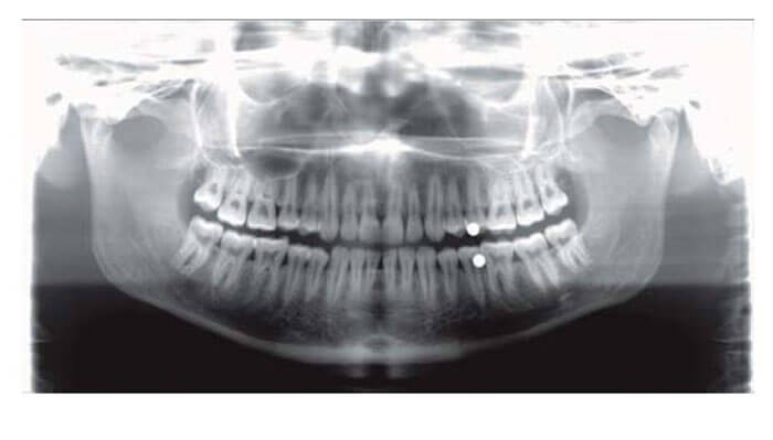
X-ray image examples
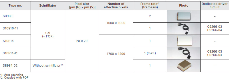
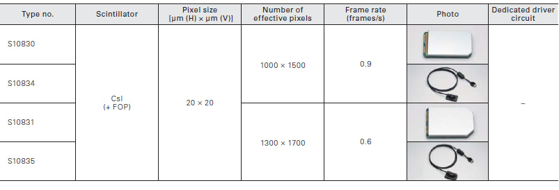
CCD area image sensors for X-ray radiography
CCD image sensors with large photosensitive area and high resolution are used in X-ray radiography.
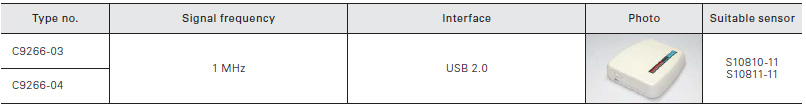
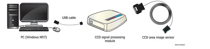
CCD signal processing module
CCD image sensors with large photosensitive area and high resolution are used in X-ray radiography.
Signal processing circuit for X-ray CCD area image sensors. Easy to use only connecting to a PC. The C9226 - 03 has a BNC connector for external trigger input.
CCD signal processing module
CMOS area image sensors for X-ray radiography
CMOS image sensors with large photosensitive area and high resolution are used in X-ray radiography.
Photosensitive area
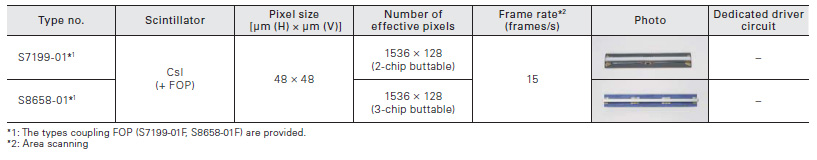
TDI-CCD area image sensors
These CCDs are long and narrow type FFT-CCD area image sensors coupling FOS. CCD chips are linearly arranged in close proximity to form a long and narrow sensor format. They are used for X-ray radiography or non-destructive inspection.
Photodiode arrays with amplifier for non-destructive inspection
Photodiode arrays with amplifier having phosphor sheet affixed on the photosensitive area are allowed for non-destructive inspection
Driver circuits for photodiode arrays with amplifier
Connection examples
Flat panel sensors are digital X- ray image sensors newly developed as key devices for rotational radiography ( CT ) and other real-time X- ray imaging applications requiring high sensitivity and high image quality. Flat panel sensors consist of a sensor board and a control board, both assembled in a thin, flat and compact configuration.
For radiography (rotational type)
These are flat panel sensors for high-speed operation.
For radiography (biochemical imaging)
These are flat panel sensors for low energy X-ray.
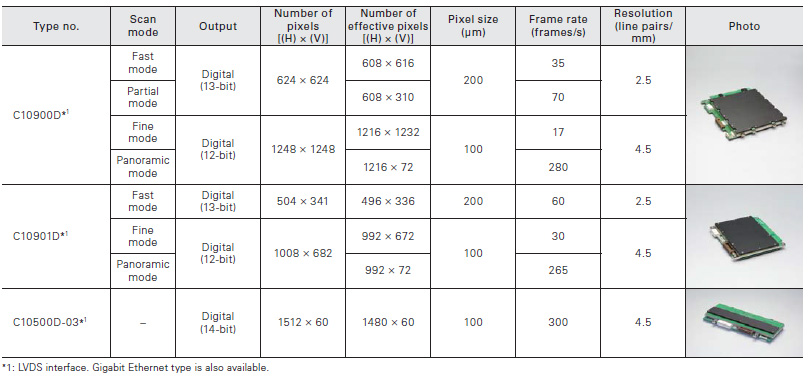
For radiography (biochemical imaging)
These are flat panel sensors for low energy X-ray.
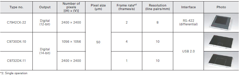
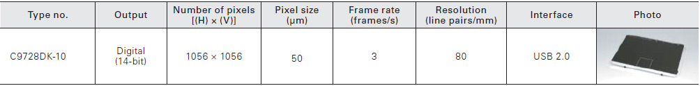
Low noise type
C9728DK-10 features low noise for application where diffraction is critical.
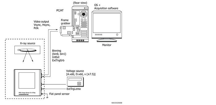
Connection example of flat panel sensors (Interface: LVDS, RS-422)
X-ray image examples
Related products for image sensors
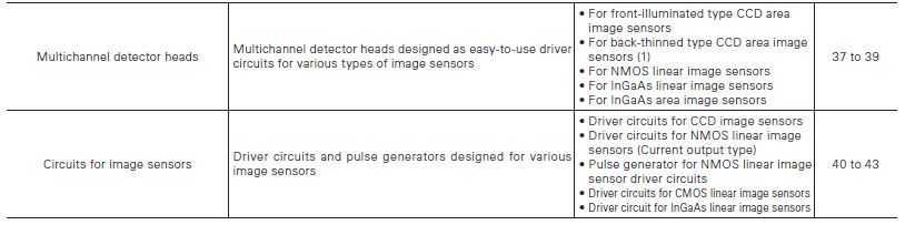
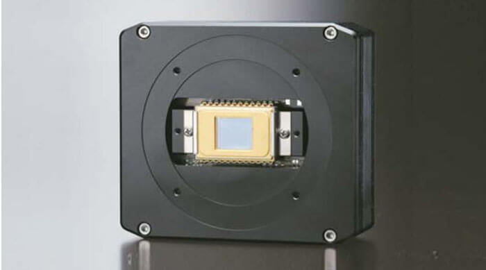
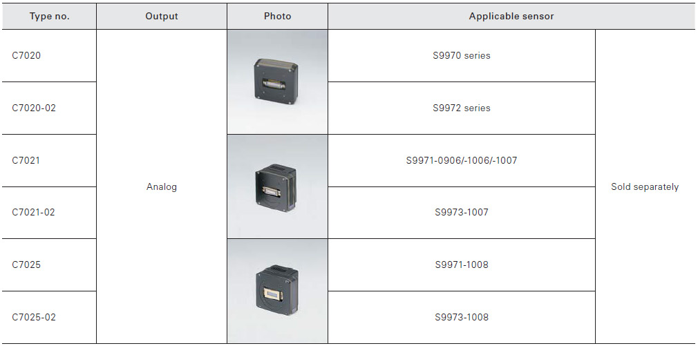
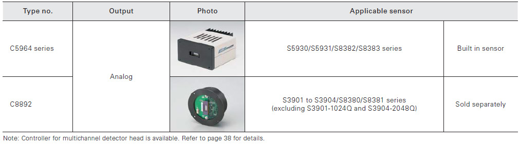
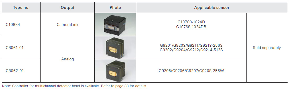
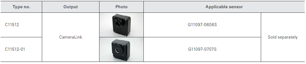
Image sensors have excellent performance characteristics, but more sophisticated electronics and signal processing are re- quired for driving image sensors than when using single-element devices. To make it easier to use image sensors, HAMAMATSU provides multichannel detector heads designed for CCD/NMOS/ InGaAs image sensors. These multichannel detector heads oper- ate with the dedicated controller or software for easy data ac- quisition and sensor evaluation and, can extract full performance from image sensors when installed in a measurement system.
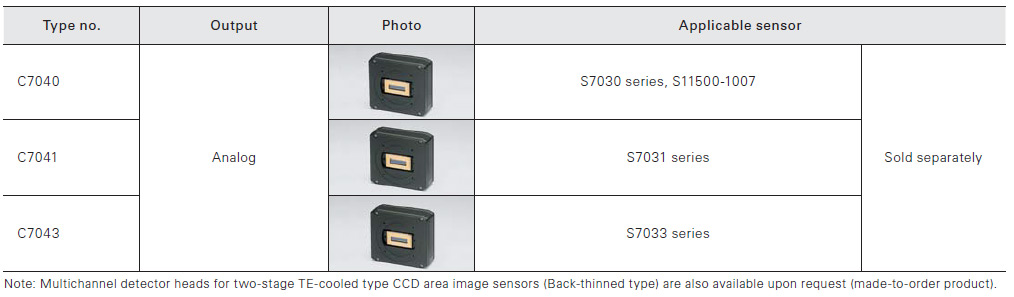
For front-illuminated type CCD area image sensors
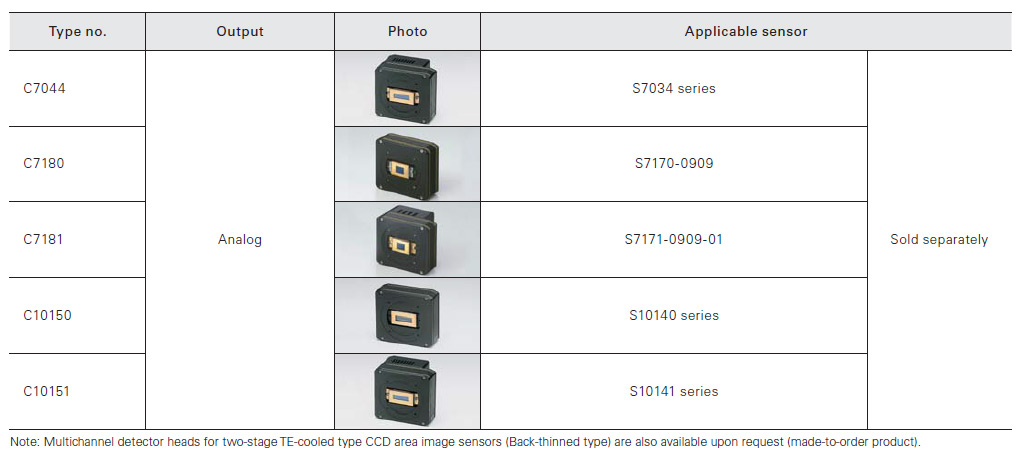
For back-thinned type CCD area image sensors (1)
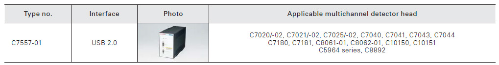
Multichannel detector head controller
Supports main multichannel detector heads designed to use a CCD image sensor or NMOS/InGaAs linear image sensor
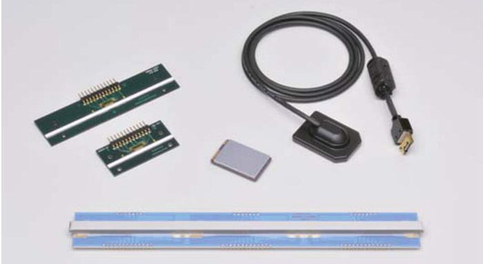
Accessories
• USB cable
• Fuse (2.5 A)
• Detector head connection cables
• AC cable
• Software [Compatible OS: Windows 7 (32- bit only)]
• Operation manual
• MOS adapter
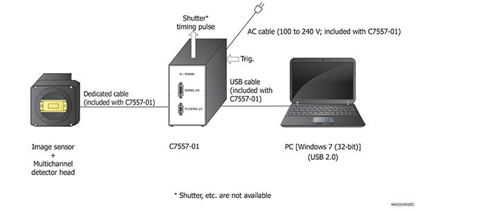
Connection examples (C7557-01)
For NMOS linear image sensors
For InGaAs linear image sensors
For InGaAs area image sensors
Driver circuits and pulse generators designed for image sensors are available.
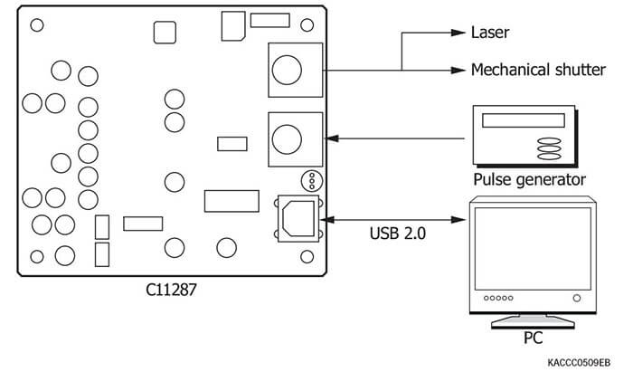
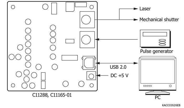
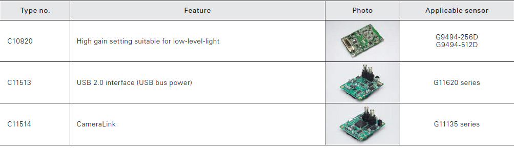
Driver circuits for CCD image sensors
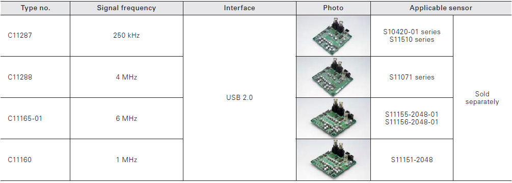
Connection examples
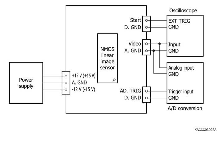
Driver circuits for NMOS linear image sensors (Current output type)
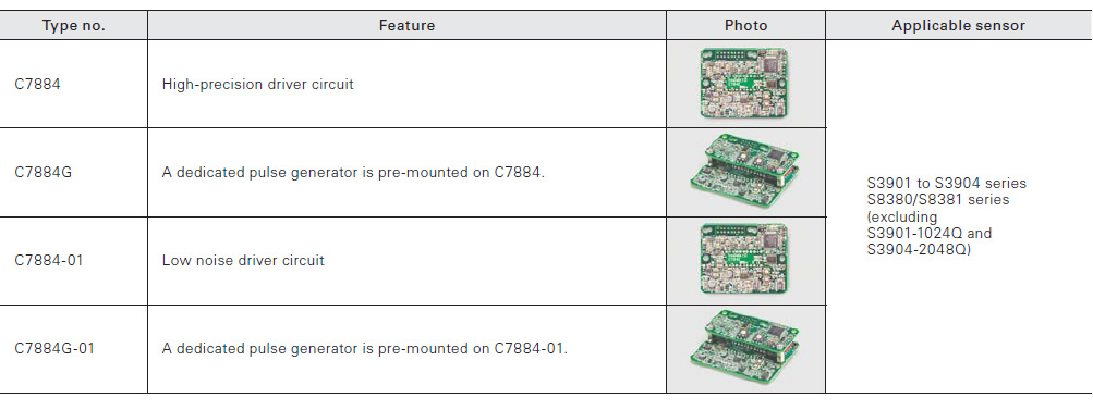
Connection examples
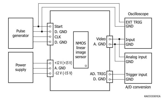
Pulse generator for NMOS linear image sensor driver circuits
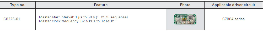
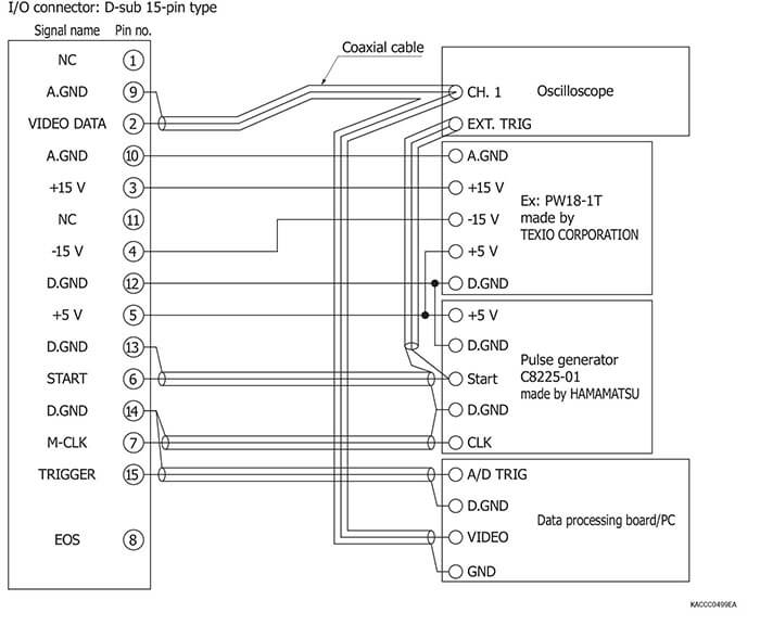
Connection example (C8225-01)
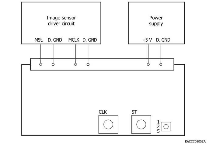
Driver circuits for CMOS linear image sensors
Connection example
Driver circuit for InGaAs linear image sensors
Connection example (C10820)
檔案下載