In-Situ Cleaning for Thin-Film Deposition

In-Situ Cleaning for Thin-Film Deposition
Staff of Kaufman & Robinson, Inc.
INTRODUCTION
Thin films are deposited on substrates in a variety of vacuum deposition processes. The properties of such a deposited film depends on the cleanliness of the substrate surface on which the film is deposited. Contamination on this surface can result in reduced adhesion of the film to the substrate, more rapid degradation of the film after deposition, greater contact resistance for electrically conducting films, and poor optical qualities for optical films.
Even with careful handling, surface contamination in the form of adsorbed water vapor and a variety of hydrocarbons results from exposure to the laboratory atmosphere prior to deposition. This exposure can also cause the formation of native oxide layers on reactive substrate materials. To remove this surface contamination, it is necessary to clean the substrate surface after it is in a vacuum environment and can no longer be contaminated by the laboratory atmosphere, but before the thin film is deposited. Glow discharges and ion beams have both been used for this in-situ cleaning.
GLOW-DISCHARGE CLEANING
A wide range of dc and rf glow discharges are used for in-situ cleaning. Equipment for dc operation is generally less costly and probably more widely used. For dc, operating voltages range from several hundred volts to several kilovolts. The most common gases for the discharge are air, oxygen, nitrogen, an inert gas, or a mixture of two or more of these. The gas pressures range from a fraction of a Torr up to several Torr.
The gas pressure for a glow discharge is usually well above the permissible background pressure for deposition, and constitutes a major limitation of glow-discharge cleaning. For a typical background pressure of 1 Torr, the mean-free-path length of a background molecule is of the order of 0.05 mm. While the path length of a more energetic ion is longer, it is still only of the order of 0.5 mm.[1] Both of these distances are quite small compared to chamber dimensions, so that diffusion of contaminants back to the surface from which they were removed is a problem. A glow discharge is also not very selective of the surfaces bombarded, so that there is an exchange of contaminants between nearby surfaces.
The redeposition that results from the high pressure and the non-selective nature of a glow discharge is probably the reason for the frequent use of oxygen, nitrogen, or a mixture that includes one or both of these. Oxygen and nitrogen are highly reactive in atomic or ionic form so that, even though the contamination is only partly removed from the substrate surface, the discharge products will react with what is left. As one example, hydrocarbon contaminants can be at least partially removed as gaseous CO and H2O by the use of oxygen in the background. As a less desirable example, an oxygen discharge can also result in the more rapid growth of an oxide layer than would occur in an atmospheric exposure.
In addition to modifying contaminants to more, or less, volatile forms, some of the glow-discharge "cleaning" probably consists of encapsulating contaminants with low-volatility deposits from elsewhere in the vacuum chamber.
When glow-discharge cleaning is completed, the high background pressure requires further pumping before the deposition of a thin film can be started. The high background pressure and the time for pumping both contribute to the accumulation of new contamination on the substrate surface before the start of deposition.
Although a glow discharge can be limited in its "cleaning" effectiveness, it can still give improved properties of deposited films, particularly in adhesion, when compared to the properties of films deposited without any in-situ cleaning.
ION-BEAM CLEANING
Both gridded and gridless ion sources[2] have been used to generate ion beams for in-situ cleaning. Gridded ion sources permit better control of ion-beam coverage, but gridless (end-Hall) sources are more cost-effective in generating the low-energy ion beams that are most frequently used for cleaning. In both cases, argon is the most common operating gas.
Ion beams have several advantages over glow discharges for in-situ cleaning. An ion beam is much more selective in that the energetic ions can be directed at a substrate, resulting in the removal of contaminants only from the substrate and
Technical Note KRI-06
immediately adjacent surfaces. The ability to vary the ion
energy independently of other parameters is also important. For removal of physisorbed contaminants such as water vapor and hydrocarbons from the laboratory environment, low ion energy are effective and energies of less than 100 eV avoid damage to, or significant sputtering of, the substrate surface. An effective cleaning dose for removal of physisorbed contaminants is quite small - less than one mA-sec/cm2.[3]
On the other hand, higher ion energies can be used for the removal of chemisorbed layers, such as native oxides. The stronger chemisorbed bonds generally require ion energies of at least 100 eV, with the required dose calculated from the sputter yield of the contaminant and its thickness.
The lower background pressure is a major advantage for ion-beam cleaning. The background pressure depends on the vacuum pumping used, but is usually in the 10-4 Torr range, resulting in mean free paths that are thousands of times longer than in glow-discharge cleaning. These longer paths greatly increase the likelihood that contaminants, once they are removed from the substrate surface, will be pumped from the vacuum chamber before they can return to that surface. The low background pressure also permits the deposition of a thin film to start rapidly after cleaning, thereby minimizing the new contamination that can accumulate between the cleaning and deposition steps. The rule-of-thumb is that a monolayer of contamination can accumulate in one second from a contaminant background pressure of 10-6 Torr. But it is important to remember that the background pressure of the contaminant is what counts, not the total background pressure which is typically almost all argon.
CONCLUDING REMARKS
In general, if the partial removal of contaminants, together with the reduction in volatility of residual contaminants, gives satisfactory properties for the films being deposited, then glow-discharge cleaning can be an acceptable, cost-effective process. But if the desired film properties require the essentially complete removal of the contaminants, rather than just modifying them to a more passive form, then ion-beam cleaning is recommended.
The preceding discussion only addresses the effects of cleaning. Depending on the deposition process and the material being deposited, ion assist during deposition can result in additional improvements in the thin-film properties.[3,4]
REFERENCES
- Staff of K&R, "Charge and Momentum Exchange in an Ion Beam," Technical Note KRI-03, 2003.
- Staff of K&R, "Broad-Beam Industrial Ion Sources," Technical Note KRI-01, 2003.
- H. R. Kaufman and J. M. E. Harper, "Ion-Assist Applications of Broad-Beam Ion Sources," Proceedings of SPIE, Vol. 5527, pp. 50-68. Aug. 2004.
-
Staff of K&R, "Ion-Assist Doses," Technical Note KRI-05, 2005, 2006.
Gas Cleanliness

Staff of Kaufman & Robinson, Inc
INTRODUCTION
Gas cleanliness is important to some vacuum-process equipment and processes. For example, contamination can decrease the lifetime of hollow cathodes and plasma-bridge neutralizers by a factor of ten or more. The techniques required to assure gas cleanliness are reviewed herein.
A typical gas-bottle installation is shown in Fig. 1. The gas is supplied from a gas bottle to a two-stage gas regulator, which decreases the pressure from the high value inside the gas bottle to about one to two atmospheres after the regulator. The gas then flows through tubing to the gas-flow valve, which may also be called a mass-flow controller. There is additional tubing from this valve to a gas feedthrough at the vacuum-chamber wall. Inside the chamber, there is more tubing from the gas feedthrough to the device that uses the gas. Gas fittings connect sections of tubing together and to other components.
GAS BOTTLE
The gas bottle should contain gas of 99.999% or greater purity. Sometimes welding-grade argon is substituted for high-purity argon. Make sure this hasn’t happened.
GAS-BOTTLE REPLACEMENT
The routine replacement of an empty gas bottle is a common cause of gas contamination. When a new gas bottle is attached to the gas regulator, a volume of atmosphere is trapped between the bottle and the regulator. Immediately opening the valve on the gas bottle will result in this trapped volume contaminating the pure gas inside the bottle.
The proper procedure is to leave the gas-bottle valve closed, pump down the vacuum system, and open all valves from the vacuum system up to the gas bottle -including fully opening the gas regulator. After the gas line is pumped out, as indicated by the vacuum chamber reaching a normal base pressure (≤1×10 6 Torr), close the gas regulator and the gas-flow valve.
Next, open the gas-bottle valve enough to show the bottle pressure on the pressure gauge before the regulator. Then open the gas regulator to give standard pressure after the regulator. If you do not have a standard pressure for use after the regulator, use 138 kPaG (20 psig). Open the gas-flow valve to give a flow of at least 10 sccm and continue for 15 minutes. This should remove essentially all of the contaminants adsorbed on the surfaces in the trapped volume between the gas bottle and the regulator and between the regulator and the gas-flow valve. Fully open the valve on the gas bottle. The gas-flow valve can then be closed. If desired, the regulator can also be closed. Proper replacement of gas bottles is necessary for gas cleanliness.
GAS REGULATOR
A high-purity, two-stage gas regulator should be used. A high-purity regulator has been cleaned ultrasonically and uses metal seals. A two-stage regulator maintains a more constant pressure, hence more stable process control.
TUBING
The total length of tubing should be minimized to reduce contamination
Technical Note KRI-04
Polymer
Polymer is used here as a generic name for a variety of plastics and elastomers. All polymers that we have tested collect impurities upon exposure to atmosphere, then gradually release these impurities at vacuum. Some polymer tubings even permit contamination to diffuse through the tube. If stainless-steel loom covers a section of tubing, you may need to check with the manufacturer to find out the tubing material. In summary, don’t use polymer tubing to transport clean gas!
Stainless Steel
Seamless stainless-steel tubing is the standard material for vacuum systems. Lubricants are used in the manufacture of this tubing. These lubricants are removed from the outside for cosmetic reasons. Unless the inside of the tubing has been cleaned, these lubricants are still there to contaminate gas for months or even years.
There are standard processes, such as electropolishing, that will clean the inside of stainless-steel tubes. Unless you know that an acceptable cleaning process has been used and the tubing was capped to keep out contamination after cleaning, assume that the inside of stainless-steel tubing requires cleaning. For long sections of tubing, there is no practical alternative to one of these standard processes. Simply rinsing the inside of a tube with a solvent is not an adequate substitute.
It is possible to clean short sections of stainless-steel tubing by hand. Use pieces of stiff wire to push through wads of lint-free tissue that have been saturated with alcohol. Repeat this process until the emerging wads show no dark residue. Rinse the inside of the tube with distilled water, then blow-dry with dry nitrogen or another clean, dry gas. Debris left inside a clean tube after cutting it should also be removed.
TUBE FITTINGS
The number of fittings should be minimized to reduce the likelihood of leaks. The fittings should be cleaned ultrasonically before being used. If ultrasonic cleaning is not available, use lint-free tissue and alcohol, followed by a rinse with distilled water and drying.
Fittings are used to connect sections of tube together or to connect tubes to other components. Different fittings have different tolerances for being opened, then reconnected. In general, any fitting connection to a gas tube should not be opened any more than necessary.
Teflon® tape should be used for threaded seals at the gas regulator. There may be a very small amount of leakage at such a joint, but the clean gas is not contaminated if the joint is kept under positive internal pressure with clean gas.
Swage-type fittings, in which the gas-tight seal is obtained by swaging a ferrule around the tube, are particularly sensitive to being opened, then reconnected. Each time a swage-type fitting is opened on the atmosphere side of the vacuum chamber, the end of the tube should be cut off, a new ferrule installed, and the fitting retightened following the manufacturer’s instructions.
Swage-type fittings inside the vacuum chamber should be considered on an individual basis. It is likely that a small leakage out of the tube to the lower pressure vacuum environment will be acceptable. In practice, few problems have been encountered due to the reuse of ferrules inside a vacuum chamber, including normal retightening without reference to the manufacturer’s instructions.
INITIAL SYSTEM PURGE
An initial purge is recommended after a gas-bottle system has been assembled using clean components. Connect a gas bottle as described above in “Gas Bottle Replacement,” except that the flow of 10 sccm or more should continued for at least an hour.
PURGE AFTER BREAKING VACUUM
Opening a vacuum chamber will expose the gas line back to the gas-flow valve to atmospheric contamination. After the subsequent pumpdown, a flow of at least 10 sccm is recommended for 15 minutes before starting operation.
A common alternate procedure is to maintain the gas flow at 10 sccm or more during the time that the vacuum chamber is open. Operation can then be started as soon as the vacuum chamber reaches a satisfactory pressure. If it is necessary to check the base pressure of the vacuum chamber, the flow can be stopped after the subsequent pumpdown reaches a pressure of less than one milliTorr.
A purge after breaking vacuum is probably the least important of the procedures described herein to assure cleanliness. It should therefore be the first procedure omitted for processes and equipment that are only moderately sensitive to gas contamination
Ion-Beam Neutralization

INTRODUCTION
As described in Technical Note KRI-01, an ion beam from a broad-beam industrial source must be neutralized. This is done by emitting electrons from a neutralizer. A hot-filament, plasma-bridge, or hollow-cathode type of neutralizer may be used. The ion source in Fig. 1 could be either gridded or gridless. For a gridless source, the neutralizer is a called a cathode-neutralizer. The target can be a sputter target or a substrate being etched. Connected to a voltmeter in Fig. 1, it serves as a neutralization probe.
RECOMBINATION
The recombination of electrons with energetic ions to obtain energetic neutrals is not a significant process at the background pressures of interest - one milliTorr or less.
The density of electrons in a broad ion beam is approximately equal to the density of ions. In plasma physics this is called “space-charge neutralization” or “quasi-neutrality.”
As an example, consider a long, cylindrical beam of 500 eV ions, 10 cm in diameter and with a current density of 1 mA/ cm2. If no electrons were present, the potential difference between the axis and the outside surface of the beam would be over 14,000 V. Such a potential difference is clearly
Cathode-neutralizer emission, A
unrealistic for 500 eV ions. For this potential difference to be reduced from over 14,000 V to 140 V, an average of about 99 electrons would be required to space-charge neutralize each 100 ions. Experimentally, the potential in an ion beam rises when there is a deficiency of electrons. At a potential relative to surrounding hardware of roughly 200 V, small arcs occur between the beam and that hardware. These arcs supply enough electrons to keep the potential from rising further. The neutralization arcs can be seen inside the vacuum chamber as 1-2 mm long flashes of extremely short duration. If the lack of neutralization is serious, the arcs will appear almost continuously on nearby hardware, giving it a sparkling appearance. These arcs can damage work pieces. If the arcs are on hardware near the work pieces, particulates can be deposited on the work pieces.
For an ion energy of <200 eV, it is more likely that the beam would become extremely divergent, or the ion source would stop operating, before the beam potential would rise enough to create these neutralizing arcs.
In summary, for an ion source operating in a normal manner, the ion beam will be space-charge neutralized. Even if the ion beam potential is sufficient to produce neutralization arcs, the departure from equal numbers of electrons and ions in each volume would be small.
Technical Note KRI-02
CURRENT NEUTRALIZATION
Current neutralization occurs when the electron emission to the ion beam is equal in magnitude to the ion current in that beam. In a gridded source, current neutralization is obtained when the neutralizer emission equals the ion-beam current. In a gridless source, it is obtained when the cathode-neutralizer emission equals the discharge current.
The effect of cathode-neutralizer emission on target potential is shown in Fig. 2 for a gridless end-Hall ion source operated at a discharge current of 5 A. The target potential was measured as shown in Fig. 1. This potential was near ground at current neutralization (-2 V), decreased moderately for excess electron emission, and rose rapidly for insufficient emission. The target had an area of only 2 cm2 and was 30 cm from the ion source. The potential variation of the target would be larger for a target that captured more of the ion beam. Regardless of the target size, though, current neutralization results in near-optimum potentials for electrically isolated targets.
PRACTICAL CONSIDERATIONS Grounded Target, Grounded Chamber Walls
If the target is electrically conducting and grounded, the neutralization requirement is moderate. Electrons are needed only to make up for the loss of the more energetic electrons that are absorbed by nearby conducting surfaces. Secondary electrons from ion collisions with grounded surfaces help make up for this loss, but it is usually necessary to have some electron emission to avoid neutralization arcs. It is recommended that the electron emission be within ±10% of current neutralization, but it is unlikely that arc-related damage would occur without a deficit greater than 50% or an excess greater than 100%.
Electrically Isolated Target, Grounded Chamber Walls
The target may be electrically isolated because it is made from a dielectric material, coated with a dielectric, or some other reason. The vacuum-chamber walls, or the sputter shields withinthosewalls,areassumedtobeconductiveandgrounded. The vacuum chamber is filled with a charge-exchange plasma (see Tech. Note KRI-03). This plasma provides an electrically conductive path from the ion beam to the walls. It is recommended that the electron emission be set between current neutralization and 10% more than this value. Any excess emission should be conducted to the vacuum-chamber walls without building up an excessive charge on the target.
Charge-Sensitive Target, Grounded Chamber Walls
This application is generally similar to the above application, except that the target is also sensitive to electrostatic charging damage [1]. As a preliminary recommendation, the electron emission should be between current neutralization and a 5% greater value. A recommended diagnostic is to measure the potential of an electrically isolated target, as shown in Fig.
1. Measuring this potential through a complete startup and shutdown cycle can be helpful in modifying procedures to reduce damage. The target potential should be maintained within ±5 V of ground, or closer if damage still occurs. It may be found from the diagnostic test that a 10-20% excess electron emission can be used without causing problems. If the beam consists of oxygen ions, the use of graphite for the diagnostic target can delay its coating with a dielectric.
Dielectric Deposition, Dielectric Coated Walls
In dielectric deposition, the dielectric is often deposited throughout the vacuum chamber. As a result, the charge-exchange plasma may not be able to provide an adequate conductive path for excess electrons, and damage may result from quite small departures from optimum electron emission. The electron emission should be set within ±5% of current neutralization. If there is any doubt about the accuracy of the metering, calibrate the meters (see Troubleshooting below). If possible, a grounded, conductive area of several hundred square centimeters should be provided near the ion source to contact the charge-exchange plasma. Such an area can be shadow-shielded from the deposition, or simply be a portion of the sputter shield that is replaced more often than the overall shield. If such a contact area can be maintained, it may be possible to both reduce work piece damage and increase the tolerance to excess electron emission.
Troubleshooting
If neutralization arcs and/or target damage are observed, but the operating condition appears reasonable, check the current meters against each other or against some common standard. Large discrepancies have sometimes been encountered with new equipment.
A hot-filament neutralizer must be located within an ion beam to provide adequate conductivity to that beam. Other neutralizer types are less sensitive to location.
Broad-Beam Industrial Ion Sources

Broad-Beam Industrial Ion Sources (Staff of Kaufman & Robinson, Inc.)
INTRODUCTION
A broad ion beam is typically several centimeters or more in diameter. The beam diameter is also much larger than the Debye length, which is the typical distance an electric field can penetrate into a plasma. If a broad beam is to be kept near ground potential, it must be neutralized (see Tech. Note KRI-02). For neutralization, there must be approximately equal numbers of electrons and positively charged ions in each volume of the ion beam. For a dielectric target, the electrons and ions must arrive in equal numbers. The target can be either a sputter target or a substrate. The ion energy in a broad ion beam is 2000 eV or less. (A singly charged ion “falling” through a potential difference of 2000 V acquires an energy of 2000 eV.) To minimize damage, the energy is usually 1000 eV or less. High energy implanting-type applications are not consider-ed here. Concern about damage to processed surfaces has led to decreased ion energies. There are two general categories of broad-beam ion sources: gridded and gridless.
GRIDDED ION SOURCES
A schematic for a gridded ion source is shown in Fig. 1, in which a dc discharge is depicted. The ions are generated by a discharge in either a circular or elongated discharge chamber. Several types of electron-emitting cathodes can be used. A hot-filament type is shown in Fig. 1. The ions can also be generated with a rf discharge, which requires no electron emitting cathode. The discharge chamber is maintained at a positive potential by the beam supply. The ions are accelerated through the apertures in the screen and accelerator grids, which are together called the ion optics.
Different grid configurations can be used. The two-grid optics shown are most common. With a dc discharge, the screen grid is close to cathode potential. With a rf discharge, the screen is connected to the positive terminal of the beam supply. Positive ions are accelerated from the positive discharge chamber, through the ion optics, to reach a target at near-ground potential. The accelerator grid is negative of the surrounding vacuum chamber (at ground) to keep electrons from the neutralizer from going backwards through the ion optics. Assuming singly charged ions, which are appropriate for this type of ion source when properly operated, the ions gain an energy in eV (electron-volts) equal to the beam-supply voltage in V.
Fig. 1. Schematic diagram of a dc gridded ion source.
Gridded ion sources operate at background pressures of about
0.5 milliTorr or less. The ion-beam output depends on the ion-optics design. The beam current increases as the grids are spaced more closely and the number of apertures is increased. The ion beam can be focused to cover a small area, collimated, or defocused to cover a larger area, depending upon the shape of the grids and the relative locations of the apertures in the grids. For given ion optics,the ion-beam current, Ib, depends on the total potential difference between the grids.
Proportionality (1) shows that the ion-beam current decreases sharply at low voltages. It may appear that a large ion-beam current can be obtained at a low beam voltage by increasing the negative accelerator voltage. But a large negative voltage can result in the ion beam spreading out so much that the ion current arriving at the target is actually decreased. Three-grid optics can reduce the beam spread at large negative voltages, but with limited effectiveness and other compromises.
Regardless of the ion optics used, a gridded ion source cannot approach the ion-current capacity of a gridless end-Hall ion source at low ion energies. The ion optics that give the superior control of ion trajectories are also the most expensive part of a gridded ion source and require the most maintenance.
GRIDlESS ION SOURCES
There are many types of gridless ion sources [2,3], but only the end-Hall and anode-layer are common in industry. The ions in a gridless source are generated by the discharge supply, with the accelerating potential difference produced by electrons from the cathode-neutralizer crossing magnetic-field lines (not shown) to reach the anode.
End-Hall Ion Source
An end-Hall ion source [2,4] is shown in Fig. 2. It has a discharge chamber that is circular or elongated. The acceleration of ions takes place in a quasi-neutral plasma, with approximately equal densities of electrons and ions. Consequently there is no limitation on ion-beam current, Ib, as expressed in Proportionality (1). The ion beam equals about 20-30% of the discharge current and the mean ion energy corresponds to about 60-70% of the discharge voltage. An end-Hallionsourceoperatesatabackgroundpressureofabout one milliTorr or less. Compared to a gridded ion source, it is reliable and rugged. It can generate large ion-beam currents at ion energies of 200 eV or less. It cannot easily generate higher ion energies and the ion-beam profile is limited to a divergent shape.
Anode-layer Ion Source
Ananode-layerionsourceisshowninFig.3. Itisalsoknownasa closed-drift ion source, which refers to the electrons precessing inaclosedpatharoundtheannularorracetrackshapeddischarge chamber. The anode-layer is a type of closed-drift source in whichmostoftheaccelerationtakesplaceinathinlayernearthe anode [3]. There are also different modes of operation for this typeofsource. Theanode-layertypeusedinindustryoperatesin
Fig. 3. Schematic diagram of anode-layer ion source.
the vacuum mode, as shown by the absence of a cathode-neutralizer [3]. The discharge voltage ranges from about 800-2000 V. The ion energies are higher than for an end-Hall ion source. This type of ion source also operates at a background pressure of several milliTorr or less [5]. The ion beam potential must be elevated to obtain neutralizing electrons from the surroundings, thus exposing the target to high electric fields and, for dielectric targets, high potentials. Target damage can therefore be a concern. Coatings on, or warping of, the pole pieces and anode can degrade performance. However, if this type of source can perform an application in a satisfactory manner, it is a very simple type of ion source.
REFERENCES
- H.R. Kaufman, “Technology of Ion Beam Sources Used in Sputtering,” J. of Vacuum Science and Technology, Vol. 15, pp. 272-276, Mar./Apr. 1978.
- H.R. Kaufman, R. S. Robinson, and R. I. Seddon, “End-Hall Ion Source,” J. of Vacuum Science and Technology A, Vol. A5, pp. 2081-2084, July/Aug. 1987.
- V.V. Zhurin, H.R. Kaufman, and R.S. Robinson, “Physics of Closed Drift Thrusters,” (Review article) Plasma Sources Sci. Technol., Vol. 8, pp. R1-R20, 1999.
-
H.R. Kaufman and R. S. Robinson, “End-Hall Ion Source,”
U.S. Patent 4,862,032, Aug. 29, 1989.
5. J.E. Keem, “High Current Density Anode Layer Ion Sources,” pp. 388-393, Proceedings SVC 44th Annual Technical Conference (2001)
Shift-Free Optical Coatings

Shift-Free Optical Coatings (Staff of Vacuum Innovations LLC )
INTRODUCTION
The deposition of optical interference coatings requires precise control of layer thicknesses and refractive indices in order to yield predictable, reliable performance. One of the challenges in the use of evaporated coatings is the porous film structure and the associated sensitivity to relative humidity and temperature which results from the low energy of the deposited molecules [1,2].
The use of an End-Hall ion source can provide added energy at the surface of the condensing film, resulting in a denser film structure for the coating molecules [3]. This denser structure can reduce or eliminate the penetration of water into the film, thereby limiting the change in refractive index and other optical parameters in the coating. This densifi cation also provides a harder, more mechanically-durable film, even at low deposition temperatures [3].
SYSTEM CONFIGURATION
A typical system for optical interference coating deposition consists of a 0.5 – 1.5m vacuum chamber with planetary or single substrate rotation and one or more evaporation sources, as shown in Fig. 1. The system geometry should be arranged to provide nearly equal coating thickness on all substrates, or masks should be introduced to partially shadow regions of higher vapor fl ux [4].
The addition of an End-Hall ion source should be configured such that nearly-equal ion flux is provided to the entire substrate surface area in the coating chamber, while maximizing the utilization of the available ion flux. The modeling of ion flux with a cosine-power distribution is discussed in KRI Technical Report TR-01. The placement of the source in the chamber and the tilt of the source from vertical provide the necessary adjustments to evenly distribute ion fl ux. The determination of ion flux uniformity requires the modeling of the substrate movement, source placement and pointing using a cosine-power distribution for the ion source flux and rotation motion for the substrate [4]. An approximate starting point is to place the source directly beneath the center of the planet and direct the source at the inner edge of the annulus described by the planet motion (see Fig.1).
ION SOURCE PARAMETERS
Successful densification of oxide materials for optical interference coatings requires operation at low ion energies and high current. Energies on the order of 100eV avoid the formation of crystallites and minimize gas incorporation,
Fig.1-Deposition chamber configuration
though the use of slightly higher ion energies (up to 150eV) may be required to achieve the desired degree of densification [5].
Development of ion-assisted deposition requires knowledge of the process variables, and the influence of each on the resulting film properties. These include the ion energy, current, gases to be used, gas flow rates, and the film deposition rate.
Ion Energy
The discharge voltage determines the ion energy (eV), by establishing the potential difference through which the ions are accelerated. On an End-Hall ion source the ion energy corresponds to approximately 60% of the discharge voltage. High discharge voltages provide greater ion energies, but can increase optical absorption and defect densities. The lowest possible discharge voltage should be utilized that achieves the desired fi lm densification, usually less than about 150V.
Ion Beam Current
The ion-beam current corresponds to about 20% of the discharge current in an End-Hall ion source. An ion beam current higher than necessary is generally not a problem [5], though the presence of a highly nonuniform distribution of ion dose may lead to significant variation in fi lm densification. A key advantage of End-Hall ion sources is the availability of high beam currents. The densification of hafnium dioxide deposited over large-area substrates in a 1.1m box coater can
Densified Hafnium Dioxide Densified Hafnium Dioxide / Silicon Dioxide Mirror Densified Hafnium Dioxide Densified Hafnium Dioxide /Silicon Dioxide Mirror
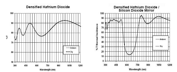
Fig.3- Influence of humidity on a 9-layer hafnia/silica mirror deposited at ambient temperature with ion-assist provided by the KRI eH3000. Once again, the difference between the film transmittance in ambient and dry envirnments cannot be resolved (fully dense).
for production throughput, while minimum rates are desired for greater densification. A suitable ion-assist process should be established with production deposition rates, reducing the rates as needed to achieve suffi cient densification.
IAD PROCESS EXAMPLE
These concepts were utilized to establish a process for ion-assisted deposition of hafnia/silica multilayer coatings in a 45-inch coating chamber with planetary rotation. Hafnia in particular requires a high ion dose for densifi cation, more than triple that required for other commonly-used oxides such as titania, tantala, and silica [7]. Hafnium metal and silica granules were used as the source materials in dual electron-beam sources. A KRI eH3000 with a hollow-cathode neutralizer was installed 11” from chamber center, pointing 15º from vertical toward the chamber center. The source was operated with a 150V/20A discharge using a 85/15 O2/Ar gas mixture for improved densifi cation. The coating process was established with no additional substrate heating, to allow processing of thermally-sensitive substrates as well as providing faster cycle times.
Initially, the aim was to establish a process for densification of hafnia. Since it is a significantly larger and higher-meltingtemperature molecule than silica, it required greater momentum and energy transfer to densify. The KRI eH3000 was operated
Fig.2- Influence of humidity on a densified hafnia layer. Note that the difference between the fi lm transmittance in ambient and dry environments cannot be resolved, indicating minimal diffusion of water in the film.
require an ion beam current up to 5A.
Gases
Ion sources typically utilize non-reactive gases such as argon, though the deposition of oxides, particularly refractory oxides such as hafnia, tantala, titania, etc., require the addition of oxygen during the deposition. The effective high-vacuum pumping speed must be sufficient to maintain the chamber pressure in the 10-4 Torr range or lower, while gases are introduced at the established process flow rates. Maintaining such a process pressure optimizes operation of the End-Hall ion source and avoids energy loss for the beam ions due to molecular collisions. Gas selection may also be used to modify the fi lm densification. For instance, the addition of a small amount (10-20%) of Ar to the O2 gas in an End-Hall source can provide significant improvements in densifi cation, since the mass of Ar is 25% greater than that of an O2 molecule. If still greater ion momentum is required, the use of Kr or Xe gases provides a substantial increase in momentum, while still using an inert gas.
Deposition Rate
The film deposition rate establishes the ion/atom ratio, which signifi cantly infl uences the fi lm densification. For a given beam current, slower deposition provides greater opportunity for the ion beam to compact the surface of the fi lm, creating a more dense coating. Maximum deposition rates are desired
Copyright © 2010 by Kaufman & Robinson, Inc., 1306 Blue Spruce Drive, Unit A, Fort Collins, CO 80524 Tel: 970-495-0187, Fax: 970-484-9350, Internet: www.ionsources.com
with a 20A discharge to provide maximum densification, but the use of 100% O2 through the source resulted in films exhibiting spectral shift given the ambient deposition temperature and large coating system. By modifying the gas flow to include 15% Ar / 85% O2, full densification of hafnia was achieved at 150V without intentional substrate heating. Spectral measurements of a hafnia single-layer coating at 40% RH and N2-purged 0% RH are shown in Fig. 2. Spectral shift is essentially eliminated through the use of the high-current eH3000, while enabling the coating to pass severe abrasion testing per MIL-C-675.
Silica can be expected to densify at lower ion source power, so ion source output may be reduced. However, it is often easier to maintain the source at constant output for all layers, provided suffi cient densification is achieved. Fabrication and testing of a 9-layer multilayer high-reflector coating was performed under identical process conditions. The use of an abbreviated high-reflector coating was utilized, since it exhibits greater sensitivity to humidity shift. The results are shown in Fig. 3.
The measurements of both the single hafnia layer and the hafnia/silica multilayer exhibit no spectral shift as the ambient humidity of the surrounding environment is varied. This indicates an absence of porosity in the fi lm, confirming suffi cient ion flux was present to fully-densify both the hafnia and silica layers without the use of substrate heating. It should be noted that operation of the ion source will lead to some heating of the substrate surface, and process development must be matched to the length of deposition and the relative thermal sensitivity of the substrate material.
CONCLUSIONS
The use of an End-Hall ion source provides high current output sufficient to fully densify hafniasilica multilayer coatings in a production-scale electron-beam deposition system. As larger area coatings are deposited in production deposition systems, the required beam current increases, necessitating the use of larger ion sources such as the KRI eH3000. Additionally, should the use of 100% O2 through the ion source prove insufficient for the degree of densification required, the use of a low fraction of a more massive gas such as Ar, Kr, or Xe may be incorporated to provide full densification at low beam voltage. Careful determination of source location and pointing can lead to uniform ion flux distribution over large substrate areas, making the integration of an End-Hall source in a production process highly effective, even for large optics.
REFERENCES
[1] J.B. Oliver et al, “Optimization of laserdamage resistance of evaporated hafnia at 351nm,” Proc. SPIE 7132 (2008).
[2] J.B. Oliver et al, “High precision coating technology for large aperture NIF optics,” in Optical Interference Coatings, OSA Tech. Digest, p. ThD2, OSA, Washington D.C. (2001).
[3] H.R. Kaufman and R.S. Robinson, “End-Hall ion source,”
U.S. Patent 4862032 (1989).
[4] J.B. Oliver and D. Talbot, “Optimization of deposition uniformity for large-aperture National Ignition Facility substrates in a planetary rotation system,” Appl. Opt. 45, 3097-3105 (2006).
[5] H. Kaufman and J. Harper, “Development and Applications of Ion Sources,” Proc. of SVC (2007).
[6] A. Anders, “Plasma and Ion Assistance in Physical Vapor Deposition: A Historical Perspective,” Lawrence Berkeley Nat. Lab. (2007).
[7] H.R. Kaufman and J.M.E. Harper, “Ion Doses for Low-Energy Ion-Assist Applications,” J. Vac. Sci. & Tech., A22 (1), pp. 221-4 (2004)
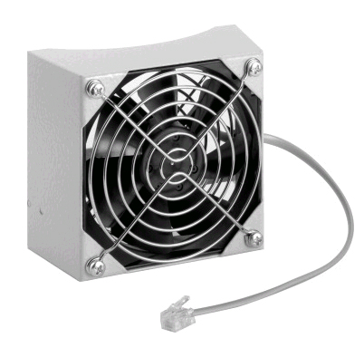
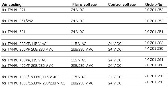
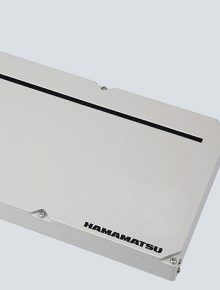
Pfeiffer 普發渦輪分子泵附件
分子泵附件 TPS 100,150,200,300,600

空氣冷卻裝置
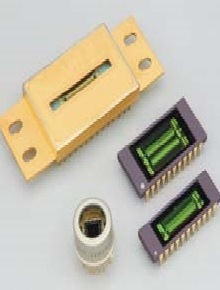
Spectroscopic modules
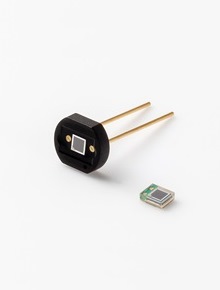
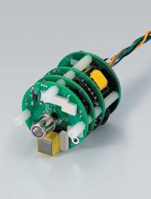
Compact module with MEMS-FPI spectrum sensor and light source
This compact module has a built-in light source, control circuit, and MEMS-FPI spectrum sensor consisting of an InGaAs PIN photodiode and MEMS-FPI (Fabry-Perot Interferometer) tunable filter which can vary its transmission wavelength by changing the applied voltage. Spectrum and absorbance can be measured by connecting a PC via USB. The product includes evaluation software with functions for setting measurement conditions, acquiring and saving data, drawing graphs, and so on. Furthermore, the dynamic link library (DLL) function specifications are disclosed, so users can create their original measurement software programs.
2D Scanning MEMs Mirror: S13124-01
The S13124-01 is an electromagnetically driven mirror that incorporates our unique MEMS (micro-electro-mechanical systems) technology. The device was made smaller by arranging the magnet beneath the mirror. A two-dimensional scanning was achieved in linear mode. Electrical current flowing in the coil surrounding the mirror produces a Lorentz force based on Fleming’s rule that drives the mirror. Hamamatsu MEMS mirrors offer a wide optical deflection angle and high mirror reflectivity.
Focusing Capillary lens - J12818-01
The J12818-01 focusing capillary lens is a focusing optics for X-rays, consisting of a bundle of numerous hollow glass capillaries formed into a cylindrical shape with its ends gently tapered. This product utilizes total reflection of X-rays on the inner wall of each capillary to focus X-rays emitted from an X-ray source to a small spot.
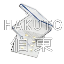
Gel-Box® 晶圓包裝盒 AD
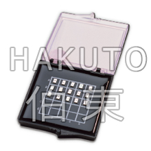
Gel-Box® 晶圓包裝盒 AD 系列
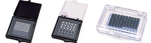
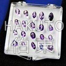
Gel-Tray® Gel 凝膠託盤 BD
Gel-Tray® Gel 凝膠託盤 BD 系列
Gel-Pak 凝膠託盤 BD 系列只提供 2”x 2” 盒子尺寸. 該託盤存儲在一個塑膠鉸鏈盒中.
Gel- pak 的專利凝膠或椎體彈性體直接應用於塑膠託盤的表面, 與晶圓包裝盒類似, 凝膠託盤產品通常手動操作, 比如使用鑷子. BD 系列提供透明的託盤,方便客戶檢查放置產品的背面
Gel-Slide™ 凝膠載玻片 CD
Gel-Slide™ 凝膠載玻片 CD 系列,CD 產品是膠膜塗在玻璃板上, 可在 80 – 220℃ 高温作业, 適合需要檢查產品背面的應用
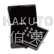
Gel-coated 珠寶盒
Gel-coated 珠寶盒
伯東公司代理美國 Gel-Pak Gel-coated 凝膠塗層珠寶盒專為固定和保護寶石, 鑽石和珠寶, Gel-Pak 專利凝膠材料固定寶石,方便編目, 儲存和運輸. Gel-Pak 珠寶盒通過寶石切面懸掛寶石, 讓光線從各個角度照射進來, 增加了珠寶的光彩
真空釋放盒 VR

可提供適用 4”, 5”, 6”, 8” 最大到 12” 晶圓存放運輸的真空釋放盒
特別適用於 GaAs / InP 晶圓以及其他大尺寸規格且易碎產品的運輸
Gel-Film 膠膜

100W 905nm Pulsed Laser Diode: L11854-336-05

75W 905nm Pulsed Laser diode: L11854-323-51

21W 905nm Pulsed Laser Diode: L11854-307-05 / -55
These LDs feature high peak power under pulsed operation. Various types are available with different peak output power and emission widths. These LDs can be used for distance measurements such as laser radar, hazard monitoring in security applications, etc.
20W 870nm Pulsed Laser Diode: L11649-120-04

21W 905nm Pulsed Laser Diode: L11348-307-05

These LDs feature high peak power under pulsed operation. Various types are available with different peak output power and emission widths. These LDs can be used for distance measurements such as laser radar, hazard monitoring in security applications, etc.
Power Supply for MPPC : C14156
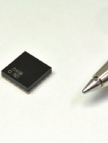
Bias power supply with built-in temperature compensation function for MPPC
The C14156 is a high voltage power supply that is optimized for driving MPPCs (multi-pixel photon counters). Up to 80 V can be output by applying a control voltage and supply voltage. It contains a temperature compensation function that constantly
optimizes the MPPC operation even in environments with varying temperatures.
Power Supply for MPPC : C11204-02
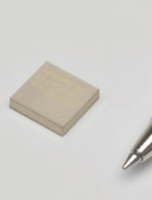
The C11204-02 is a high voltage power supply that is optimized for MPPCs (multi-pixel photon counters). It can output up to 90 V. It contains a temperature compensation function that constantly optimizes the MPPC operation even in environments with varying temperatures. It also has built-in output voltage monitor and output current monitor. All functions can be controlled from a PC via its serial interface (UART). The C11204-02 is compact and surface mount type of the C11204-01.
Power Supply for MPPC : C11204-01
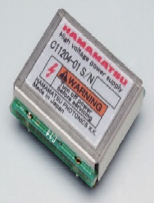
The C11204-01 is a high voltage power supply that is optimized for MPPCs (multi-pixel photon counters). It can output up to 90V. It contains a temperature compensation function that constantly optimizes the MPPC operation even in environments with varying temperatures. It also has built-in output voltage monitor and output current monitor. All functions can be controlled from a PC via its serial interface (UART).
VIS MPPCs
For wide dynamic range : S14160 series
For PET scanners: S14160 / S14161 series
For precision measurement: S13360 series
TSV type for precision measurement : S13360 / S13361 series
Cooled type for precision measurement : S13362 series
□1mm channel type: S13165 series
For visible light: S14420 series
Cooled type for visible light: S14422 series
NIR MPPCs
VUV / UV MPPCs
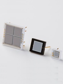
For VUV light detection
For Cherenkov telescope experiments
Photon counting module: C14076-01
Fiber coupling type, low-light-level detection
The C14076-01 is a photon counting module that can detect low-level light. It consists of a TE-cooled single pixel photon counter (SPPC), amplifier, comparator, high-voltage power supply circuit, and temperature controller. This product is a fiber coupling type module. The module operates by supplying an external power supply (±5 V). As this product is compact and lightweight, it is suitable for integration into devices.
Photon counting modules: C11202 series
Single pixel photon counting module for low-light-level detection
The C11202 series is a single-photon counting module capable of detecting low light levels. The C11202 series is made up of a thermoelectrically cooled single-pixel photon counter (SPPC), an amplifier, a comparator, a high-voltage power supply circuit, and a temperature controller. The photosensitive area is available in two sizes of ϕ50 μm and ϕ100 μm, and such small photo- sensitive areas offer a low dark count. Modules operate just by connecting them to an external power supply (±5 V).
pinhole inspection unit for pouch rechargeable batteries: C15477
By making use of a photomultiplier tube with a large photosensitive area and a noise-suppression signal processing technique, Hamamatsu Photonics has developed a new pinhole inspection unit, the model C15477 that quickly finds pinhole defects as small as 1 micron (millionth of a meter or μm hereafter) in diameter in sheet workpieces. This new product can detect tiny pinhole defects only a quarter of the size of pinholes detectable up to now, and so will improve inspection accuracy for tasks such as inspecting pinhole defects in fuel cell separators for fuel cell vehicles and aluminum laminate films for pouch rechargeable batteries. This product is available as a set with a light source unit and a light collector unit optimized for inspecting pinhole defects in sheet workpieces such as large thin metal sheets measuring 480 mm wide by 180 mm deep.
SCAN BLOCK: C10516
Compact scan head for easy assembly into a system
An optical block that combines galvano scanners with a telecentric fθ (F-theta) lens designed for laser beam scanning in the visible range. 21.5 mm diameter observation area. Full measurement systems such as a laser scanning fluorescence, reflecting, or confocal microscope can be made by coupling this block to other optical blocks. High magnification images can be observed with a photomultiplier tube by attaching the scan block to the C-mount port of a commercial microscope.
2D Laser Scanning MEMs mirror: S13989-01H
mini-Spectrometer SMD series: C14384MA-01
High sensitivity in the near infrared region (to 1050 nm), ultra-compact grating type spectrometer
The C14384MA-01 is an ultra-compact grating type spectrometer head that provides high sensitivity in the near infrared region. As such, it is capable of acquiring continuous spectrum. The head has been downsized through Hamamatsu unique optical design, which helps to further reduce the size of mobile devices.
RADIATION LINE SENSOR C13247
The C13247 is an energy differentiation type radiation line sensor designed for an efficient, non-invasive detection of pipe corrosion in industrial plants such as oil, gas and petrochemical refineries. The C13247 ensures high accuracy that never seen up till now and reliable inspections of pipe corrosion.
In conventional visual and ultrasonic inspections, the heat insulator materials must be removed from around the pipes. This also requires the time and the cost of installing scaffolds to remove and rewrap the heat insulator materials. Other techniques that utilize conventional radiation inspection or neutron moisture measurement have the problem of being easily affected by scattered radiation which makes accurate measurement difficult.
The C13247 energy-discriminating radiation line sensor solves all of these problems to successfully capture sharp, clear inspection images.
FTIR engine C15511-01
The C15511-01 Fourier transform infrared spectrometer (FTIR) engine is compact enough to carry in just one hand. A Michelson optical interferometer and control circuit are built into a palm-sized enclosure. Spectrum and absorbance can be measured by connecting a PC via USB. It can be applied to real-time measurement performed on site without bringing the measurement sample into the analysis room as well as continuous monitoring.
The optical interferometer has a built-in light input section, beam splitter, fixed mirror, movable mirror (ϕ3 mm), and photodetector. The photodetector acquires light intensity signals that vary depending on the position of the movable mirror. The optical spectrum is obtained by processing (Fourier transform) these light intensity signals.
The FTIR engine has a built-in semiconductor laser (VCSEL: vertical cavity surface emitting laser) for monitoring the movable mirror position, which allows spectrum measurement with high wavelength accuracy.
The product includes evaluation software with functions for setting measurement conditions, acquiring and saving data, drawing graphs, and so on. Furthermore, the dynamic link library (DLL) function specifications are disclosed, so users can create their original measurement software programs.
OPTICAL PINHOLE INSPECTION UNIT FOR LAMINATE FILM AND FOILS: C12570
LIGHTNINGCURE UV-LED spot light source LC-L1V5 : L14310
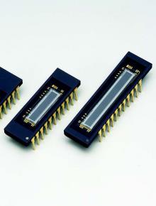
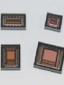
NMOS linear image sensor
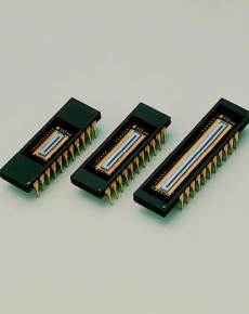
CCD linear image sensor
CMOS linear images sensor
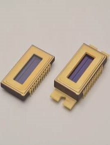
Front-illuminated type CCD area image sensor
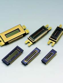
CMOS area image sensor
Back-thinned type CCD area image sensor
X-ray image sensor
Multichannel detector head
Image Sensors for Near Infrared Region
Distance image sensors
Photodiode Arrays with Amplifier
Micro-spectrometer C12666MA
Compact 2W Xenon Flash Lamp Module : L13821
Compact 2W Xenon Flash Lamp Module : L13651
WATER-COOLED TYPE DEUTERIUM LAMP : L1314; L1835
COLLIMATING CAPILLARY LENS : J12432-01
OPTICAL BLOCKS
MEMS mirror : S12237-03P
FAC LENS (Fast-Axis Collimating Lens) : J10919 SERIES

Compact and thin, built-in high-sensitivity CMOS image sensor for Raman spectroscopy : C13054MA
Ultra-compact mini-spectrometer integrating MEMS and image sensor technologies : C10988MA-01
0.3毫米 (0.012英寸)
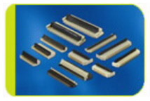
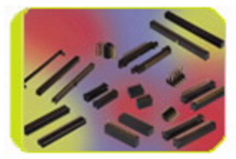
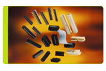
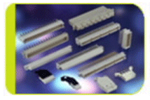
FCI提供全套系列的0.3毫米间距连接器,用于板上空间较小的应用。FCI的0.3毫米间距连接器拥有13 - 51位。
0.2毫米(0.008英寸)
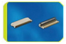
FCI提供间距为0.20mm的非常矮型的弹性接头,可为PCB板节省空间。
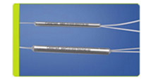
波分复用器

多模星状耦合器
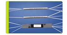
Canstar公司的NxM耦合器具有多模模式,使用户可以通过多路光纤同时传输和分配同一数据。这些多模耦合器可在600至1600nm以外和在400至700nm的可见光以内工作。各种不同的光纤规格对应不同的应用,包括50/125/250µm(电信标准)、62.5/125/250 µm(数据通讯标准)、100/140/171 µm(军事与航空)和200/240/500 µm及以上(传感器、医疗和工业应用,包括电力传输/配电系统-如HVDC(高压直流电))。
分光器和耦合器

Canstar 公司1x2和2x2 单模耦合器设计用于测试设备及光纤网络。通过特许使用熔融双锥形耦合器专利,经过专业改进和严格的质量控制,即使在恶劣的环境条件下也能实现最佳的性能与操作。单模耦合器适用于单或双窗口设计的特定波长(850、980,1300、1310或1550nm)。使用SMF(TM)光纤的耦合器适用于大于1250nm(9/125/250)的波长,而Hi-Index/Bend-Insensitive光纤适用于小于1250mm的波长。
无源光学元器件
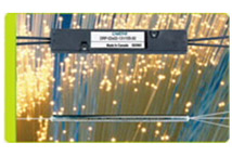
1978年,Canstar公司开发出熔融双锥形(FBT)光耦合器技术,从此以后,Canstar公司一直成为光纤行业的引领者。自此,Canstar便成为光耦合和光纤技术的代名词。从Canstar公司成为FCI公司的一部分时起,我们就通过开发、生产及提供专门设计的无源光纤解决方案以稳定不变的质量标准为配电、仪表、军用航空市场、电信和医疗/健康市场客户服务,以帮助他们提供高性能的信号分配系统。所有的Canstar产品均符合RoHS标准。FCI 连接器(Canada)股份有限公司通过CGP认证(列管货物计划)。
电缆组件
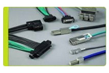
FCI 是电缆组件互连解决方案的领先供应商。我们提供广泛系列的产品,旨在为高速信号、电源和光纤传输提供支持。
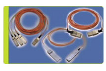
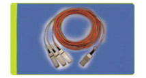
光纤电缆组件

FCI光纤制造采用最先进的设备和光学设计技术,为客户提供附加值解决方案。为满足或超过行业标准,FCI对适用性能参数终端进行了100%的测试,这些性能参数包括插入损耗、回波损耗、顶点偏移、曲率半径和底切。适用标准包括TelcordiaGR-326-CORE和客户特殊要求。
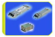
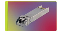
收发器

FCI提供一系列光学收发器,其包括一系列行业标准和MSA标准产品,从XFP和SFP+到引入的PCB板空间节省型收发器,例如提供小巧外形(SCFF)产品。提供的产品符合各种高速工业应用标准,包括以太网到10Gb/s以太网、2/4/8Gb/s 和 10Gb/s FibreChannel、无限带宽QDR 和各种IEEE 802.3技术规范。
收发器
FCI提供一系列光学收发器,其包括一系列行业标准和MSA标准产品,从XFP和SFP+到引入的PCB板空间节省型收发器,例如提供小巧外形(SCFF)产品。提供的产品符合各种高速工业应用标准,包括以太网到10Gb/s以太网、2/4/8Gb/s 和 10Gb/s FibreChannel、无限带宽QDR 和各种IEEE 802.3技术规范。
有源光缆
有源光缆(或AOC’S)具有最佳的链路性能、高可靠性和互操作性以及安装便利.由于其设计特点,AOC没有任何外露的光纤接口,从而排除了污染风险。FCI提供CXP对CXP、QSFP+对QSFP+AOC’S以及CXP对3QSFP+分路电缆。这些电缆非常适用于数据中心设备,为线架对线架、集群对集群以及中心对中心转换应用提供即插即用的光纤解决方案,每根电缆的总带宽达150 Gb/s,从而优化端口密度。为补全所提供的产品,FCI还提供外形为CXP、QSFP+和SFP+的铜基直接连接电缆(DAC)。
波分复用器
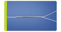
Canstar单模波分复用器设计用于合并和分离测试设备、光纤传输设备和系统中的两个光信号。980/1550 nm波分复用器专门设计用于EDFA系统。通过特许使用熔融双锥形耦合器专利,经过专业改进和严格的质量控制,即使在恶劣的环境条件下也能实现最佳的性能与操作。
多模星状耦合器

分光器
Canstar 公司1x2和2x2 单模耦合器设计用于测试设备及光纤网络。通过特许使用熔融双锥形耦合器专利,经过专业改进和严格的质量控制,即使在恶劣的环境条件下也能实现最佳的性能与操作。单模耦合器适用于单或双窗口设计的特定波长(850、980,1300、1310或1550nm)。使用SMF(TM)光纤的耦合器适用于大于1250nm(9/125/250)的波长,而Hi-Index/Bend-Insensitive光纤适用于小于1250mm的波长。
适配器
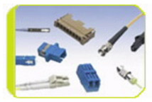
FCI光纤制造采用最先进的设备和光学设计技术,为客户提供附加值解决方案。为满足或超过行业标准,FCI对适用性能参数终端进行了100%的测试,这些性能参数包括插入损耗、回波损耗、顶点偏移、曲率半径和底切。适用标准包括TelcordiaGR-326-CORE和客户特殊要求。
组件

FCI光纤制造采用最先进的设备和光学设计技术,为客户提供附加值解决方案。为满足或超过行业标准,FCI对适用性能参数终端进行了100%的测试,这些性能参数包括插入损耗、回波损耗、顶点偏移、曲率半径和底切。适用标准包括TelcordiaGR-326-CORE和客户特殊要求。
SCFF型收发器
FCI的FCI P/N-TRX08GVP2540型SCFF光学收发器造型小巧(SCFF),基于行业标准SFP+型采用机械方式改进而成。其设计目的在于与现有的SFP=标准比较,在不影响性能或线板密度的情况下,可节省大量内板空间。其11个插脚电气接口符合高速接口(包括与I2C接口和电源类似的2线串行接口)SFP+ MSA(SFF-8431)规范。根据《2002/95/EC指令》,该收发器符合RoHS 6/6标准;根据IEC/CDRH标准,它符合激光安全1类标准。该收发器功耗不足一瓦,结构紧凑,使得系统设计时具有较高的端口密度。该收发器配有双工LC光纤接口,以用于光纤电缆连接。
XFP收发器
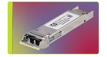
FCI公司的XFP收发器完全符合XFP MSA 4.5修订版标准,并支持基于以太网、光纤信道(FibreChannel)及IEEE 802.3ba的应用。收发器具有SR(波长:850mm)配置,非常适用于单信道(每个I/O端口)数据通讯和存储网络传输应用。每个收发器都配有用于光缆的双工LC光纤接口。为补足所提供的产品,FCI还提供XFP板连接器、外罩以及匹配光纤LC双工电缆组件
SFP+ 收发器
QSFP - QSFP AOC's

有源光缆(或AOC’S)具有最佳的链路性能、高可靠性和互操作性以及安装便利。FCI公司的QSFP+对QSFP+有源光缆组件中的每根电缆都有4个全双工信道,每个信道可支持的信号传输速率高达10 Gb/s。由于其设计特点,AOC没有任何外露的光纤接口,从而排除了污染风险。QSFP+电缆接口以SFF-8436行业标准为基础,同时满足40GBASE-SR4以太网和无限带宽SDR、DDR 和 QDR 标准的要求。QSFP+电缆在使用时属于非导电性、Plenum级和螺旋型8芯多模光纤电缆,允许任何方向的电缆路由选择和弯曲度。这些电缆适用于高密度信号传输,在大多数数据中心和高性能计算应用中非常常见
CXP-3xQSFP AOC
有源光缆(或AOC’S)具有最佳的链路性能、高可靠性和互操作性以及安装便利。FCI公司的CXP对3QSFP+有源光缆组件中的三根4信道分支电缆共有12个全双工信道,每个信道可支持的信号传输速率高达12.5Gb/s。由于其设计特点,AOC没有任何外露的光纤接口,从而排除了污染风险。CXP电缆接口以SFF-8642和无限带宽行业标准为基础,而QSFP+接口符合SFF-8436标准。CXP对C3QSFP分支电缆在使用时属于非导电性、 Plenum级和螺旋型24芯多模光纤电缆,允许任何方向的电缆路由选择和弯曲度。这些电缆适用于高密度信号传输,在大多数数据中心和高性能计算应用中非常常见。
CXP-CXP AOC
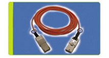
有源光缆(或AOC’S)具有最佳的链路性能、高可靠性和互操作性以及安装便利。FCI公司的CXP对CXP有源光缆组件中的每根电缆都有12个全双工信道,每个信道可支持的信号传输速率高达12.5Gb/s。由于其设计特点,AOC没有任何外露的光纤接口,从而排除了污染风险。CXP电缆接口以SFF-8642和无限带宽行业标准为基础。CXP对CXP电缆在使用时属于非导电性、Plenum级和螺旋型24芯多模光纤电缆,允许任何方向的电缆路由选择和弯曲度。这些电缆适用于高密度信号传输,在大多数数据中心和高性能计算应用中非常常见。
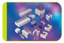
1.25mm 间距 WtB 连接器系统
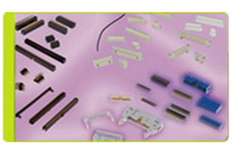
间距1.25mm板系统的延长线,适用于涉及PCB板有线连接的各种应用。
1.27mm 间距 BtB/WtB 连接器系统
Minitek127® 是一种广泛应用于各种线对板和缆对板应用的模块型连接器。它包括平角和直角,可表面贴装和通孔安装,有多种电镀法和多达100多个位置。
Quickie® 2.54 mm
Quickie® 是FCI品牌,为2.45mm间距的缆线对板连接器。 quickie® 产品系列包括IDC插座、IDC板用连接器、带盖低矮型插头和带盖弹出式锁扣插头
PV® 2.54mm线对板连接器系统
创新型 PV® 压接线系统将离散的电线与印刷电路板相连。高可靠性双金属插座端子插头与行业标准的0.025英尺(0.635mm)接线柱相连。各种密封、保护和导向选件适用于连接器界面的两侧
Minitek™ 2.00 mm
Minitek™ 是FCI品牌,为2.00间距的板对板和导线/缆线对板连接器。Minitek™产品系列包括PCB卡连接器、带盖插头、无盖插头和IDC/CTW插座。连接器适用于表贴、通孔、引脚浸锡膏法安装,双排型,4至50位平角或直角方向。每个触点的最大额定电流值为2A。
Dubox™ 2.54 mm
Dubox™连接器系列提供种类繁多的通孔和表贴零件选择,包括自2至50位呈直角或平角方向的单排或双排,每个触点的额定电流值(最大值)为3A。 Dubox™ 触点具有预加应力的双线束设计,确保信号保护所需的较小插入力和4壁触点设计。
Bergstik® 2.54 mm
BergStik® 产品系列适用于表贴、通孔和引脚浸入锡膏型安装,可提供2至72位呈平角或直角方向的单排或双排产品。各连接器具有“脱离”设计,能通过剪切或折断的方式调整其长度,以适合应用模型。 每个触点的最大额定电流值为3A。
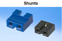
Shunts

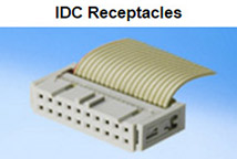
IDC Receptacles
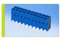
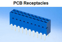
PCB Receptacles
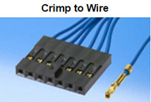
Crimp to Wire
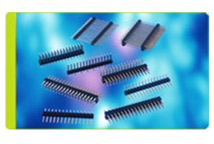
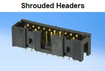
Shrouded Headers
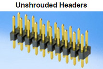
Unshrouded Headers


Xcede 6 对
1.可提供4、6、8柱选择
2.产品的可用性包括低于 25 G/ bps运行的高速选项或 低于 10 G/bps运行的低速选项
3.有2个压接EON配置选项
4.可作为一个单一的独立装置提供,或以单块组装方式提供,在单个组件中配有任何数量的其他信号、电力和指导选项
5.可提供8585Ω或100Ω配置
6.针对Telcordia GR -1217核心中央办公室,基于性能进行电镀测试
7.Amphenol TCS的第2个源,可以相互配对、在电子和机械上实现互换
Crossbow正交型
1.速度高达20Gb/秒
2.4对和6对垂直插头和直角插座
3.用于高速交换和数据通信应用
Xcede背板
FCI 的XCede® 连接器平台设计拥有25 Gb/s传输速率性能,以支持下一代数据中心和服务供应商网络设备对未来高速, 串行数据传输速率的要求。在共振阻尼防护罩内使用工程聚合物,可使得宽频带内的串音极低。
XCede 连接器也可满足背板和子卡接口对较高线性信号密度的要求,可提供多达82.4差分对/英寸。 晶片整理器可将直角信号、引导和功率模块组合,形成一个集成的子卡连接器。
Metral ®HDXS
1.基于输入/输出连接器系统的Metral架构(IEC 61076-4-104)
2.符合VDSL要求 - 24对和72对配置
3. 符合 ITU-T K20 (ANSI 2.5kV)关于连接器和板上空间的要求。
4. 如需了解详细信息,请联系
DIN 41612 核心产品选择器
Millipacs®核心产品选择器

1.IEC 61076-4-101
2.5+2和8+2排模块化系统
3.紧凑型 PCI
4.硬公制互连系统
5.符合硬公制制造惯例的高速选项:Airmax VS® 和 Zipline™
METRAL®Core,2.00毫米间距(0.79英寸)
1.IEC 61076-4-104
2.4、5和8排模块化系统
3.焊接到板、通孔回流焊或压接终端式样
4.高速选项: Metral® HS
“发明家们”设计出完善的METRAL®连接器系列
AirMax VS® 共面,Zip Line®共面
FCI 的 AirMax VS® 和 ZipLine® 高性能连接器系统还支持共面板之间的高速连接。直角插座与插头连接器能够在 ATCA® 系统中的前板和后端传输模块之间实现共面扩展卡应用或第 3 区连接。
产品具有灵活的每列差分对数量,能够满足对于信号密度、连接器外形或气流的需求。AirMax VS 连接器配置有每列 15 个触点(5个差分对),列间距为 2 毫米,每英寸拥有 63.5 个差分对,并且卡槽...
![]() +886-2-8772-8910
+886-2-8772-8910